• Acta Photonica Sinica
  • Vol. 51, Issue 5, 0551302 (2022)
Aiping LIU1, Guangjie CHEN2, Liang CHEN2, Xinbiao XU2, Yanlei ZHANG2, Qin WANG1, and Changling ZOU2、*
Author Affiliations
  • 1Institute of Quantum Information and Technology,Nanjing University of Posts and Telecommunications,Nanjing 210003,China
  • 2CAS Key Laboratory of Quantum Information,University of Science and Technology of China,Hefei 230026,China
  • show less
    DOI: 10.3788/gzxb20225105.0551302 Cite this Article
    Aiping LIU, Guangjie CHEN, Liang CHEN, Xinbiao XU, Yanlei ZHANG, Qin WANG, Changling ZOU. Advances in Integrated Photonic-atom Chips(Invited)[J]. Acta Photonica Sinica, 2022, 51(5): 0551302 Copy Citation Text show less

    Abstract

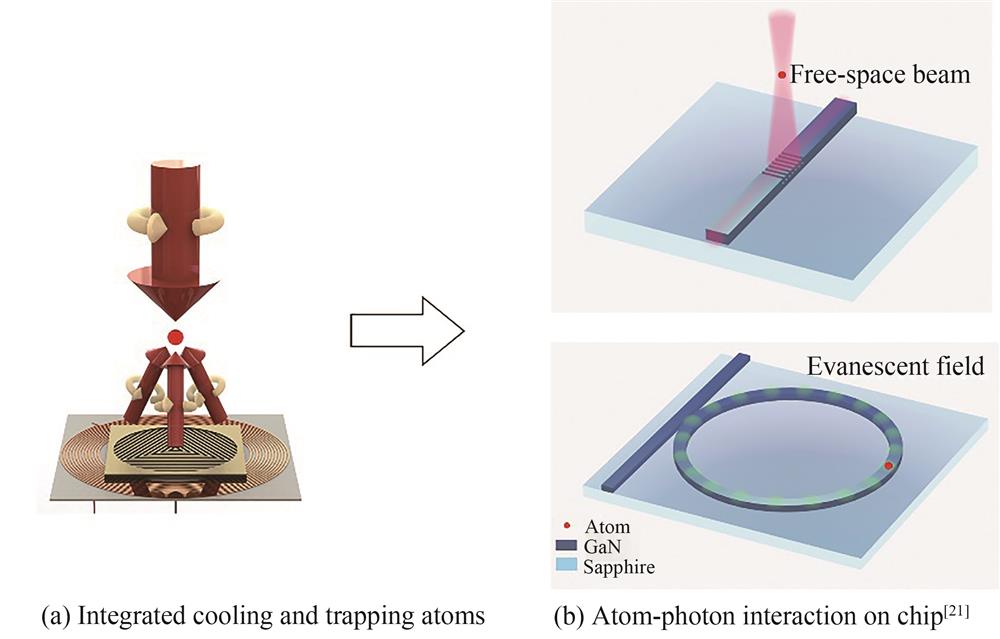
    In recent years, exciting progress are made in the research of micro-nano optical devices and integrated optical chips, which promotes the combination of various optics-related research fields and integrated optical technology. Atomic physics has also achieved great success in the last decades and had found applications in sensing, time-keeping, the search for new physics, and also the emerging quantum information sciences. Thanks to the close relationship between optics and atomic physics, the combination between the atomic physics and the integrated photonics chip allows a new research field of the photonic-atom chip, which holds the advantages of both research fields and holds the potential for portable atomic systems and also for the scalable quantum information processing platform.In this paper, the development of this research field is reviewed. In general, the development of the photonic-atom chip could be divided into two paths. The first path is the chip-integrated magneto-optical trap and dipole traps in free space. Utilizing the compact multi-functional diffractive components and also chip-to-free space interfaces, the neutral atoms could be cooled, trapped, manipulated, and also read out by the structured optical fields in free space. Since the conventional bulky optical devices could be replaced by photonic chips, and thus the size of experimental setups for the atomic system could be greatly reduced. The second path focus on the near-field interaction between atom-photonic structures. By trapping and conveying the cold atoms to the surface of the photonic chip, the single atoms could be trapped by the evanescent field of integrated waveguides and microresonators. Due to the strongly localized optical fields on the chip, the light-atom interaction could be greatly enhanced. Therefore, the photonic-atom chip could not only reduces the power consumption for atom trapping and transporting, but also allows the high-fidelity atom-photon entanglement, the manipulation, and readout of atomic quantum states, which promises the single photon-single atom quantum interfaces for potential quantum information processing units.In the past two decades, attention has been attracted to the new research direction of the photonic atom chip, and great progress has been achieved in both theoretical and experimental aspects. In particular, this field lies at the intersections of photonics, atomic physics, and quantum information science. Now, the compact chip-integrated magneto-optics trap, single-atom trapping, and the detection of a single atom by integrated microresonators have been demonstrated. In this paper, we reviewed these exciting progress following the two distinct paths, focusing on either the free-space structural optical field or the near-field of the photonic micro-/nano-structures.Although great efforts are dedicated to this field, only the principle of key photonic-atom chip devices are demonstrated, and we could envision that there are still several years to go to really apply these devices in applications. We want to point out the following perspective research topics. 1) The single-atom array on a photonic chip. By either confining single atoms on an array of microresonators or trapping the single atoms by the tweezer array generated by on-chip diffractive devices, a stable array of single atoms is promising. 2) The integration of multiple functional devices to form a fully-functional hybrid photonic-atomic integrated circuits. By incorporating mature photonic devices, including the high-efficient frequency doubler, high-speed electro-optic modulator, and GHz-frequency acousto-optics modulators, into the photonic-atom chip, the more complex and novel atom-based applications could be developed. 3) The realization and manipulation of atomic matter-wave. We can imagine that the trapped atoms in the straight or bent waveguides could be treated as the matter-wave propagating along the waveguides, thus potential circuits of atom matter wave could be realized. Combining the atom-photon interaction in the same waveguide, these novel photonic and matter-wave circuits could be utilized for matter-wave applications, such as the inertial sensor.
    Aiping LIU, Guangjie CHEN, Liang CHEN, Xinbiao XU, Yanlei ZHANG, Qin WANG, Changling ZOU. Advances in Integrated Photonic-atom Chips(Invited)[J]. Acta Photonica Sinica, 2022, 51(5): 0551302
    Download Citation