
Shuai Cui, Kaixiang Cao, Zhao Pan, Xiaoyan Gao, Yuan Yu, Xinliang Zhang. Compact microring resonator based on ultralow-loss multimode silicon nitride waveguide[J]. Advanced Photonics Nexus, 2023, 2(4): 046007
- Advanced Photonics Nexus
- Vol. 2, Issue 4, 046007 (2023)
Abstract
1 Introduction
The past decades have witnessed dramatic progress in the development of photonic integrated circuits in silicon-on-insulator. Silicon (Si) has been the mainstream platform of integrated photonics,1 with the key advantages including large-area substrates, and mature and high-yield complementary metal oxide semiconductor (CMOS)-compatible fabrication. Tremendous effort, such as sophisticated fabrication processes and a highly multimode structure, has been made to improve the -factor of Si photonic resonators.2,3 However, the propagation loss still cannot be reduced sufficiently low. The main reason is the two-photon absorption of the telecommunication wavelengths has drastically restricted its applications to occasions requiring low propagation loss at high power, such as tunable lasers4 and optical frequency combs.5 To address this challenge, silicon nitride () has emerged as an attractive CMOS-compatible alternative to integrated photonics.6
Several approaches have been proposed to achieve ultralow propagation loss in waveguides. A propagation loss as low as or even lower than 11,18
In this work, we propose and demonstrate an ultrahigh racetrack resonator based on a uniform multimode waveguide, even without any special fabrication process. The multimode waveguide, which refers to the waveguide width that is far beyond the single-mode regime, is used to reduce the contact between the optical field and the rough sidewall, thus reducing the scattering loss of the optical waveguide. The microring resonator (MRR) consists of two adiabatic Euler bends and two multimode straight waveguides (MSWs). Multimode directional couplers (DCs) are used to achieve the adiabatic propagation of the fundamental mode and suppress the excitation of higher-order modes in the racetrack. With the help of Euler bends and a DC, a compact footprint resonator with a large FSR, ultralow loss, and low intermode coupling is achieved. The high- resonator is fabricated with simple standard 800-nm- multi project wafer (MPW) foundry processes. Notably, the racetrack resonator is made of a -wide uniform waveguide, and the perimeter is only 2.226 mm, corresponding to an FSR of . Compared with previously reported results,30 the mean intrinsic of the MRR is increased by more than 5 times higher order and reached 10.8 million for the first time, and the corresponding propagation loss is estimated to be about . Our method of using highly multimode structures to achieve ultralow propagation loss can be applied to other material platforms. It can potentially be applied to optical frequency combs, microwave photonic filters, and optoelectronic oscillators.
Sign up for Advanced Photonics Nexus TOC. Get the latest issue of Advanced Photonics Nexus delivered right to you!Sign up now
2 Device Design
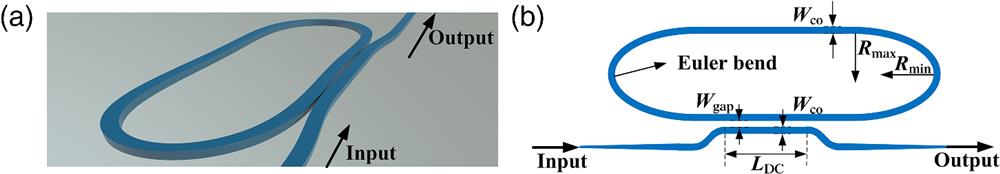
Figures 1(a) and 1(b) show the three-dimensional (3D) and the top views of the designed ultrahigh racetrack resonator based on a uniform multimode waveguide. The racetrack MRR is composed of two MSWs and two multimode waveguide bends (MWBs) based on modified Euler bends. Although the waveguide width of the Euler bends is far beyond the single mode, the Euler bends can guarantee adiabatic transmission for the fundamental mode with low intermode cross talk, ultralow excess loss, and a compact footprint. No higher-order modes are excited in the MRR. A DC is used to couple the light from the bus waveguide to the MRR. Notably, the DC is realized using two MSWs with the same width. By controlling the coupling length and the coupling gap, the optical coupling only occurs for the fundamental mode, and higher-order mode excitation is suppressed.
![]()
Figure 1.Schematic diagram of the proposed compact ultrahigh-
Figure 2(a) shows the cross section of the waveguide, whose core width is broadened to weaken the optical sidewalls’ interaction and thus reduce the light scattering loss at the sidewalls significantly. The wafer is with an 800-nm-thick layer and a -thick buried-oxide layer. A -thick thin film is deposited on the top as the upper cladding. The interaction between the optical field and the rough sidewalls is responsible for distributing the scattering loss. Here, we use an model to analyze the scattering loss, which provides a comprehensive analysis of the fundamental role played by the sensitivity of the effective index of the optical mode to waveguide width variations.31 This approach enables an accurate description of practical optical waveguides and provides simple design rules for optimizing the waveguide geometry, thus reducing the scattering loss generated by rough sidewalls. According to the design rules of LIGENTEC AN800 Technology (LAT), the propagation loss is for the standard waveguide with a cross section of . The relationship between waveguide width and scattering loss can be predicted by the model. From Fig. 2(b), it can be seen that when the standard deviation of the roughness and the correlation length () of the rough sidewalls are determined, the scattering loss decreases with the increase of waveguide core width . This happens because when the waveguide core becomes wider, the optical field at the sidewalls of the waveguide becomes weaker. We can also see that when is larger than , the scattering loss is not very sensitive to the increase of . Further, as the waveguide width increases, the MRR footprint will consequently increase. Therefore, to balance the bending radius and the waveguide loss, the waveguide width is designed to be .
![]()
Figure 2.Design of the compact ultrahigh-
Figures 2(c)–2(d) show the mode profiles in the 1- and wide waveguides, which are simulated by the finite-difference Eigenmode method provided by Lumerical MODE Solutions. We can clearly see that when the waveguide width is , the contact between the (TE = transverse electric) mode and the rough sidewalls is much less than when the waveguide width is . Thus, the scattering loss caused by the rough sidewalls is significantly reduced. According to the model shown in Fig. 2(b), the estimated scattering loss of the waveguide ( and ) are 0.18 and when the waveguide widths are 1 and , respectively. Therefore, the value of the MRR can be significantly boosted.
To ensure the fundamental mode to be transmitted in the ring adiabatically, the MWBs should be carefully designed to avoid exciting higher-order modes. To achieve high integration density as well as a large FSR, the MWBs with modified Euler bends are used in the MRR. The modified Euler curve means that the curvature varies linearly along the length of the curve and can provide a high degree of adiabaticity and compact footprint. The Euler bend is defined as2
As shown in Fig. 1(b), the 180 deg bend comprisesf a pair of 90 deg Euler bends. Notably, the maximal radius should be large enough to ensure negligible mode mismatch at the junction between the MSW and the MWBs, and should be chosen to ensure adiabatic transmission. We simulate the mode field in the -wide waveguide and find that the lowest four modes (, , , and ) can all be well supported. Using the 3D finite-difference time-domain (FDTD) simulations (Lumerical FDTD), we simulate and calculate the mode excitation ratios (MERs) of the higher-order modes at different and , and find that when and , the calculated MERs, such as , , and , are all below in the broadband from 1500 to 1600 nm, as shown in Fig. 2(e). Therefore, the cross talk of the higher-order modes calculated in the MWR can be ignored. It should be noted that the waveguide height is , which can also support transverse magnetic (TM) mode transmission. Therefore, we also calculate the MERs of higher-order TM modes excited by mode, as shown in Fig. 2(f). The calculated MERs of , , and excited by mode are all below in the broadband from 1500 to 1600 nm. Therefore, the cross talk of the higher-order modes of the TM mode can also be ignored.
Figure 2(g) shows the simulated light propagation field in the 180 deg Euler MWBs when and . The corresponding mode profile at the input, the quadrant MRR (), and the output of the 180 deg Euler MWBs are shown in Fig. 2(h). It can be seen that almost no multimode interference is observed, which indicates that the designed Euler MWBs work very well. Meanwhile, the optical field is well confined in the -core region and has little interaction with the sidewalls. For the designed MWBs, the effective radius of the ring is calculated to be only . A multimode MRR with a constant large radius of is proposed with a cross section of .24 For this MRR, it is also difficult to reduce the bending radius due to intermode coupling. In contrast, the proposed racetrack resonator is made of a -wide uniform multimode waveguide, with an effective radius as small as .
In addition, the DC-based multimode waveguides should also be carefully designed to ensure adiabatic coupling for the fundamental mode. To ensure sufficient coupling for the fundamental mode and avoid exciting the higher-order modes, the coupling length of the multimode DC of the MRR should be long enough, and the coupling gap should be sufficiently small. By choosing and the length of DC , we can obtain the simulated light propagation in the multimode DC from the racetrack to the bus waveguide, as shown in Fig. 2(i). It can be seen that no higher-order modes are excited in our designed multimode DC. It should be noted that the waveguide width is far beyond the single-mode regime and can support multimode transmission in the optical waveguide.32 When light propagates along the waveguide beyond the single-mode regime, higher-order modes can be excited and thus induce undesired mode-mismatching loss as well as intermode cross talk. Thanks to the designed adiabatic coupler and Euler bend, only the fundamental mode is excited and transmitted in our designed resonator.
To summarize, the adiabatic transmission process of mode is as follows. First, the mode is input into the bus waveguide, and the mode is adiabatically coupled to the MRR by the specially designed multimode DC. Then, the mode undergoes adiabatic transmission in the MWBs, and finally, the mode is adiabatically coupled from the MRR back to the bus waveguide. In the designed MRR, the power cross-coupling ratio of the DC is 0.006, and the perimeter of the MRR is .
3 Device Fabrication and Measurement
Figure 3 shows the false color image of the fabricated compact ultrahigh racetrack resonator. All the devices in this work are fabricated by the MPW foundry (LIGENTEC, Switzerland) with the standard processes of deep ultra-violet (DUV) lithography. Figure 3(a) shows the global view of the resonator with a size of . The microscopic images of the modified Euler bend, the adiabatic taper, and the DC are shown in Figs. 3(b)–3(d), respectively. Figure 4 shows the experimental setup for characterizing the factor of the fabricated ultrahigh racetrack resonator, which maps the bandwidth of the MRR from the optical domain to the electrical domain.33 The optical carrier emitted by a tunable laser source (TLS, NKT Basik E15) is input into a phase modulator (PM, Covega Mach-40) via a polarization controller (PC1). Then the phase-modulated light is launched into an optical bandpass filter (OBPF). One of the first-order sidebands of the modulated signal is eliminated by the OBPF and then a single sideband (SSB) signal can be obtained correspondingly. The remaining sidebands of the generated SSB signal are used to scan the resonant notch to obtain the transmission spectrum of the racetrack microring. Then the light is amplified by an erbium-doped fiber amplifier and coupled into the chip via PC2, which is used to adjust the state of polarization (SOP) of the light to the chip. A pair of tapered optical fibers (OMT-APC-TJ-1M), which are fixed by flip-top fiber optic clamps (OMFG06, OMTOOLs), are used to couple the light into and out of the device under test. Then the SSB signal is launched into the chip. After being filtered by MRR, the output signal is routed to a high-speed photodetector (PD, SHF AG-Berlin) with a bandwidth of 40 GHz. Finally, a microwave photonic notch filter (MPNF) is obtained, and the transmission of the ultra-high resonator is mapped to the transmission of the MPNF. Therefore, the transmission of the ultrahigh resonator can be measured by a vector network analyzer (VNA, Anritsu MS4647B) precisely.
![]()
Figure 3.False color images of the fabricated ultrahigh-
![]()
Figure 4.Experimental setup for characterizing the
In this section, we characterize the FSR and factor of our designed and fabricated ultrahigh- MRR. Since precise frequency calibration is required to measure the FSRs, we adjust the wavelength of the TLS carefully to expand the measurement range to several FSRs of the MRR (see Appendix). From Fig. 5(a), it can be seen that both the TE and TM modes exist in an FSR. This is because the thickness of the waveguide is , which also supports TM mode transmission. The FSR of MRR is simply defined and calculated as34
![]()
Figure 5.Measured results of the MRR (height
To investigate the performance of the designed ultralow-loss multimode waveguide, we analyze the propagation loss of the waveguide beyond the single-mode regime by the following equations:34
Table 1 shows the comparison of recently reported ultrahigh resonators that have a higher than . The first three MRRs with a high factor are achieved by low-confinement waveguides and fabricated based on the ultralow-loss high-aspect-ratio (H-A-R) waveguide technology. It can be seen that all of the propagation losses are lower than . However, all of the bending radii are very large and result in small FSRs, which restricts the application scenarios and is still not conducive to highly dense integration. Notably, devices based on high-confinement waveguides can overcome these challenges. Recently, there have been some reports of ultralow loss and high-confinement waveguides based on the traditional subtractive process and photonic Damascene process. However, the key to achieving low propagation loss all include introducing complex fabrication processes solely to minimize the scattering points at the waveguide interfaces, such as reflowing resist masks,11,25,27 multipass lithography,19,28 and optimizing the etch recipe.10,19 These special fabrication techniques are nonstandard and incompatible with those standard processes in foundries. Notably, all of the reported high- MRRs are fabricated in laboratories, not for the MPW. Therefore, it is still greatly desired to achieve low-loss optical waveguides using the MPW, such as the standard LAT process. According to Ref. 37, the propagation loss of the fabricated waveguides based on LAT is . In contrast, using our proposed high multimode structure, the propagation loss is successfully reduced from 20 to . Correspondingly, the fabricated racetrack resonator can achieve a mean as high as 10.8 million, and the FSR is as large as 65.0 GHz. The high- MRRs can be applied to many fields, such as optical soliton sources,38 high-coherence/low-threshold Brillouin lasers,39 optical frequency combs,40 microwave photonic filters,33 and optoelectronic oscillators.41
| Reference | ( | Manufacturing process | Propagation loss (dB/m) | |||
| 2014 | 11.0 × 0.04 | H-A-R | 0.32 | 9.65 | ||
| 2021 | 8.0 × 0.10 | H-A-R | 0.1 | 0.95 | ||
| 2021 | 11.0 × 0.04 | H-A-R | 0.06 | 11.787 | ||
| 2020 | 2.1 × 0.95 | Photonic Damascene process | 1.4 | 2.3 | — | |
| 2021 | 2.2 × 0.95 | Photonic Damascene process | 1.0 | — | — | |
| 2022 | 2.2 × 0.95 | Photonic Damascene process | 2.4 | — | — | |
| 2021 | 2.6 × 0.73 | Subtractive process | <1 | 0.147 | — | |
| 2021 | 1.9 × 0.74 | Subtractive process | — | — | — | |
| 2023 | 2.4 × 0.81 | Subtractive process | 2.6 | — | — | |
| 2021 | 0.8 × 0.8 | Standard LAT process | 20 | 0.5 | — | |
| This work | 3.0 × 0.80 | Standard LAT process | 3.3 | 0.195 |
Table 1. Comparison of reported high-
4 Conclusion
In summary, we have proposed and demonstrated an ultrahigh- MRR based on a high multimode waveguide. The waveguide width is optimized by the model to reduce the scattering loss. A multimode waveguide-based DC is used to achieve adiabatic coupling for the fundamental mode and avoid higher-order mode excitation simultaneously. At the same time, the modified Euler multimode bending is employed to reduce the size and avoid exciting higher-order modes in the MRR simultaneously. Therefore, adiabatic coupling and adiabatic propagation for fundamental mode in multimode waveguides are achieved to ensure fundamental mode resonance. Thanks to the adiabatic DC and Euler bends, although the multimode waveguide width of the MRR is as wide as with , only the fundamental mode is excited and transmitted in the MRR with ultralow loss, and higher-order modes are successfully suppressed. Compared with previous MRRs fabricated based on the same LAT process, our proposed high multimode waveguide can reduce the propagation loss from previous 20 to . Correspondingly, the intrinsic is increased from previous reported 2 to 10.8 million. The high multimode design can be applied not only to but also to different material platforms. In principle, these high multimode structures can be further combined with sophisticated optimized fabrication processes to reduce propagation loss. The proposed approach opens wide opportunities for applications in microwave photonics, classical and quantum information processing, and ion sensing.
5 Appendix: Measuring the FSR of MRR
We perform a microwave photonic link, as shown in Fig. 4, to measure the ultrahigh- resonator transmission through VNA. As the bandwidths of PD and PM are both 40 GHz, the measuring range of the VNA is also set to be 40 GHz, which corresponds to a wavelength range of 0.32 at 1550 nm. Considering that the FSR of the ultrahigh- resonator is as large as , the measured frequency response of the MPNF by VNA must be spliced. Taking Fig. 5(a) as an example, at first the wavelength of the TLS is adjusted to 1549.77 nm, and the OBPF is adjusted to eliminate the +1st-order sideband of the phase-modulated light. Then, the transmission of the microresonator from 1549.77 to 1550.09 nm can be measured by VNA. The next step is to adjust the wavelength of the TLS to 1550.09 nm, and the OBPF is also adjusted correspondingly to eliminate the +1st-order sideband of the phase-modulated light. Then, the transmission of the microresonator from 1550.09 to 1550.41 nm can be measured by VNA. Finally, the transmission spectra of and mode as shown in Fig. 5(a) can be obtained by splicing the two measured transmission spectra by VNA.
Shuai Cui is currently pursuing his PhD at Wuhan National Laboratory for Optoelectronics, Huazhong University of Science and Technology (HUST), Wuhan, China. His current research interests include microwave signal processing and microwave signal generation.
Kaixiang Cao is currently pursuing his master’s degree at Wuhan National Laboratory for Optoelectronics, HUST, Wuhan, China. His current research interests include microwave signal processing and microwave signal generation.
Zhao Pan is currently pursuing his master’s degree at Wuhan National Laboratory for Optoelectronics, HUST, Wuhan, China. His current research interests include microwave signal processing and microwave signal generation.
Xiaoyan Gao is currently pursuing his doctoral degree at Wuhan National Laboratory for Optoelectronics, HUST, Wuhan, China. His current research interests include microwave signal processing and microwave signal generation.
Yuan Yu received a PhD in optoelectronic information engineering from the School of Optical and Electronic Information, HUST, Wuhan, China, in 2013. He is currently an associate professor at Wuhan National Laboratory for Optoelectronics and Institute of Optoelectronics Science and Engineering, HUST. His current research interests include microwave photonics and silicon-based integrated devices.
Xinliang Zhang received a PhD in physical electronics from HUST, Wuhan, China, in 2001. He is currently a professor at Wuhan National Laboratory for Optoelectronics and the School of Optical and Electronic Information, HUST. He is the author or coauthor of more than 300 journal and conference papers. His current research interests include InP-based and Si-based devices and integration for optical network, high-performance computing, and microwave photonics.
References
[4] C. Calò et al. Hybrid InP-SiN microring-resonator based tunable laser with high output power and narrow linewidth for high capacity coherent systems(2022).
[8] A. L. Gaeta et al. Photonic-chip-based frequency combs. Nat. Photonics, 13, 158-169(2019).
[41] L. Maleki. The optoelectronic oscillator. Nat. Photonics, 5, 728-730(2011).

Set citation alerts for the article
Please enter your email address
© Copyright 2018-2021 | Chinese Laser Press. All Rights Reserved 沪ICP备15018463号-20