
Xuerui Sun, Yinan Wu, Chuanyi Lu, Yuting Zhang, Hao Li, Shijie Liu, Yuanlin Zheng, Xianfeng Chen, "Experimental investigation on the unbalanced Mach–Zehnder interferometer on lithium niobate thin film," Chin. Opt. Lett. 20, 101301 (2022)
- Chinese Optics Letters
- Vol. 20, Issue 10, 101301 (2022)
Abstract
Keywords
1. Introduction
Integrated photonics on lithium niobate thin film (LNTF) has emerged as an outstanding approach for on-chip scalable optical signal manipulation and processing, which has attracted widespread attention and stimulated tremendous enthusiasm in recent years[
As one critical component among integration applications, the Mach–Zehnder interferometer (MZI), which can be balanced or unbalanced, has a wide range of applications. Amplitude modulators based on the balanced MZI structure are ubiquitous and play a significant role in optical switching, processing, and communication[
Here, we report on an optimized UMZI designed and fabricated in LNTF via electron beam lithography (EBL) and inductively coupled plasma (ICP) etching. A high extinction ratio (ER) of 32.4 dB and a low extra loss (EL) of 1.14 dB are obtained on the basis of the total interferometer. Both the thermo-optic and electro-optic tunability of the fabricated UMZI is experimentally investigated. A linear tuning efficiency of 42.8 pm/°C and 55.2 pm/V is obtained. The demonstrated structure has applications for sensing and filtering in PICs on the novel platform.
Sign up for Chinese Optics Letters TOC. Get the latest issue of Chinese Optics Letters delivered right to you!Sign up now
2. Device Design, Fabrication, and Characterization
In our design, the UMZI on
![]()
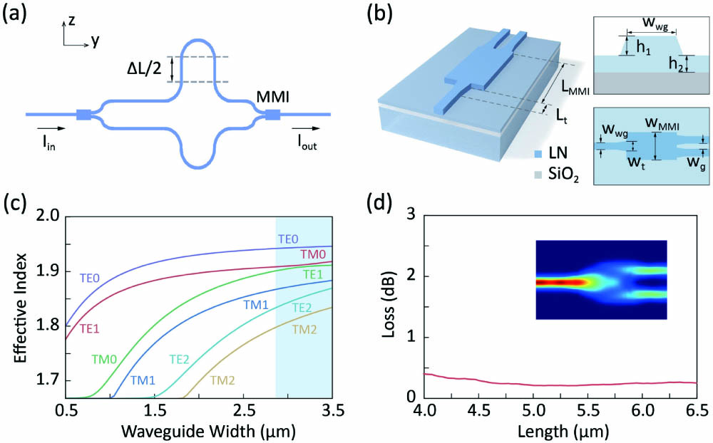
Figure 1.(a) Schematic of the UMZI with a length difference of ΔL. MMI, multimode interference coupler. (b) Schematic of the MMI from different view angles. (c) Calculated effective index neff of optical modes versus the ridge waveguide width with an air upper cladding. (d) Calculated loss of the MMI with respect to its length. The MMI width is 2.80 µm.
Figure 1(c) shows the calculated effective index
In our experiment, the UMZIs, together with referencing MMI couplers and straight waveguides, are fabricated by EBL and ICP etching techniques on the same LNTF sample. The fabrication procedure starts from a commercial
The integration of compact MMI beam couplers and low-loss waveguides is important in high-performance MZIs. Firstly, the loss of individual MMI couplers is experimentally investigated, where a straight waveguide is used as a reference. The MMI coupler shows low loss in a wide span, as shown in Fig. 2. The wavelength span is limited by the used tunable laser in our experiment. The experimental EL is less than 1.5 dB over the whole span, with a loss of roughly 0.4 dB at 1550 nm. The calculated loss is about 0.2 dB over a broad band starting from 1500 to 1600 nm.
![]()
Figure 2.Experimentally measured EL of the MMI coupler. Inset: optical microscopy image of the MMI coupler.
3. Results and Discussion
Other than the well-proportioned splitting ratio of the MMI couplers, both arms of the MZI are bent to balance the extra bending loss in order to achieve a high ER. Figure 3 shows an optical microscopy image of the fabricated UMZI. A straight waveguide is used as reference to measure the EL of the UMZI. Light is coupled into the waveguide through grating coupling. It should be noted that the grating coupler itself has a high degree of polarization dependence. The input/output grating coupler is optimized for the TE mode only, so TM modes experience a large loss in the device. The grating couplers have a period of 0.85 µm and a duty cycle of 0.33 for maximum efficiency at the wavelength of 1550 nm. The SEM image of the grating coupler is shown in the upper left inset of Fig. 3(a). The upper right inset shows the SEM image of the compact 50:50 MMI components with a length of 5.31 µm and a width of 2.80 µm. To reduce the coupling loss between the fiber and the waveguide, an adiabatically tapered waveguide is manufactured to connect the interferometer and the grating coupler. Figure 3(b) is the SEM image of the cross-sectional view of the nanowaveguide. The top width of the fabricated ridge waveguide is 700 nm with an etching depth of about 325 nm, with an etched sidewall inclination angle of about 65 deg. Figure 3(c) indicates the simulated electric field distribution of the
![]()
Figure 3.(a) Optical microscope image of the UMZI. Insets: SEM images of the grating coupler and MMI components, respectively. (b) False-color SEM image of the cross section of the ridge waveguide. (c) The simulation of the fundamental TE mode at 1550 nm.
An amplified spontaneous emission (ASE) light source centered at 1550 nm with a 50 nm bandwidth is used to measure the spectral response of the UMZI at room temperature. The normalized transmission spectrum of the TE-polarized light is shown in Fig. 4(a). The achieved ER in the whole span of ASE ranges from 20 to over 30 dB. A high ER of 32.4 dB is achieved at the wavelength of 1539.5 nm. The high ER of the individual UMZI without cascading configuration indicates that the split ratio of the MMI couplers is close to the ideal parameter, and bending loss is well balanced. This is comparable with the highest demonstrated ER on LNTF to date[
![]()
Figure 4.Normalized transmission spectrum of the fabricated UMZI.
To characterize the thermal tunability, we measured normalized transmission spectra of the UMZI at different temperatures. The result is displayed in Fig. 5(a). As can be seen, a temperature variation from 20°C to 70°C causes a total redshift of the spectrum by 2.14 nm. The FSR at different temperatures is marked as demonstrated in Figs. 5(b) and 5(c), inferring negligible variance. Figure 5(c) also shows that the normalized transmission spectra exhibit a highly linear shift with a slope of 42.8 pm/°C. More efficient control approach of thermo-optic tuning may rely on metal micro-heaters[
![]()
Figure 5.(a) Thermo-optic tuning performance of the UMZI. (b) The FSRs of the UMZI at temperatures from 20°C to 70°C. (c) Wavelength shift and FSR as a function of the temperature. (d) The measured output power varying with temperature and its fitting curve at 1534.34 nm.
The output versus the varying input power at room temperature is investigated to demonstrate the stability of the UMZI under high optical powers, as displayed in Fig. 6(a). The wavelength corresponding to the peak transmitted power is approximately 1560.7 nm. The dependence of the maximum output power and the corresponding wavelength on the input is shown in Fig. 6(b). The wavelength is nearly unchanged with the increase of the input power, except for a tiny shift at 60 mW. Notably, the UMZI performs stably at large input optical powers, due to ultralow propagation loss of the nanowaveguides.
![]()
Figure 6.(a) Measured transmitted optical spectrum analyzer (OSA) spectra as a function of input power. (b) Maximum output signal and its wavelength versus input power.
As presented above, the UMZI on LNTF can achieve a comparatively large ER and a relatively low EL. Modulation based on the UMZI can also utilize the electro-optic effect of LN, which is important in optical modulators, electric field sensing[
Furthermore, active tuning is also implemented through the electro-optic effect. For electro-optic tuning, the UMZI is similar to the previous one. The arm path of the unbalanced MZI is extended by 2 mm, and the path difference is kept the same. A gold electrode with a thickness of 200 nm and a spacing of 6 µm (with a 20-nm-thick Cr adhesive layer) is deposited to one arm of the UMZI. The length of the electrode is 2 mm. The image of the sample is not shown in the figure. The electric field is applied along the
![]()
Figure 7.(a) Electro-optical tuning performance of the UMZI. (b) The FSRs of the UMZI at voltages from 20 V to 45 V. (c) Wavelength shift and FSR as a function of the voltage. (d) The measured output power varying with voltage and its fitting curve at 1549.3 nm.
4. Conclusion
In summary, we report on the design and fabrication of UMZIs on LNTF via EBL and ICP etching processes. The UMZIs experimentally achieve a high ER of 32.4 dB and an EL of 1.14 dB in the telecommunication band. A linear shift with a tuning slope of 42.8 pm/°C and 55.2 pm/V is obtained by harnessing the strong thermo-optic and electro-optic effects of LN. The working wavelength of the UMZI is almost independent of the incident power, which verifies the ultralow propagation loss of the waveguides. The UMZI can be used as a basic structure for a variety of optical components in PICs to achieve wide applications.
References
[1] A. Boes, B. Corcoran, L. Chang, J. Bowers, A. Mitchell. Status and potential of lithium niobate on insulator (LNOI) for photonic integrated circuits. Laser Photonics Rev., 12, 1700256(2018).
[2] J. Lin, F. Bo, Y. Cheng, J. Xu. Advances in on-chip photonic devices based on lithium niobate on insulator. Photonics Res., 8, 1910(2020).
[3] D. Zhu, L. Shao, M. Yu, R. Cheng, B. Desiatov, C. J. Xin, Y. Hu, J. Holzgrafe, S. Ghosh, A. Shams-Ansari, E. Puma, N. Sinclair, C. Reimer, M. Zhang, M. Lončar. Integrated photonics on thin-film lithium niobate. Adv. Opt. Photonics, 13, 242(2021).
[4] Y. Qi, Y. Li. Integrated lithium niobate photonics. Nanophotonics, 9, 1287(2020).
[5] Y. Zheng, X. Chen. Nonlinear wave mixing in lithium niobate thin film. Adv. Phys., 6, 1889402(2021).
[6] D. N. Nikogosyan. Nonlinear Optical Crystals: A Complete Survey(2006).
[7] C. Wang, M. Zhang, X. Chen, M. Bertrand, A. Shams-Ansari, S. Chandrasekhar, P. Winzer, M. Lončar. Integrated lithium niobate electro-optic modulators operating at CMOS-compatible voltages. Nature, 562, 101(2018).
[8] M. Xu, M. He, H. Zhang, J. Jian, Y. Pan, X. Liu, L. Chen, X. Meng, H. Chen, Z. Li, X. Xiao, S. Yu, S. Yu, X. Cai. High-performance coherent optical modulators based on thin-film lithium niobate platform. Nat. Commun., 11, 3911(2020).
[9] M. Li, J. Ling, Y. He, U. A. Javid, S. Xue, Q. Lin. Lithium niobate photonic-crystal electro-optic modulator. Nat. Commun., 11, 4123(2020).
[10] M. Xu, M. He, Y. Zhu, L. Liu, L. Chen, S. Yu, X. Cai. Integrated thin film lithium niobate Fabry–Perot modulator [Invited]. Chin. Opt. Lett., 19, 060003(2021).
[11] X. Liu, B. Xiong, C. Sun, J. Wang, Z. Hao, L. Wang, Y. Han, H. Li, J. Yu, Y. Luo. Wideband thin-film lithium niobate modulator with low half-wave-voltage length product. Chin. Opt. Lett., 19, 060016(2021).
[12] K. Abdelsalam, E. Ordouie, M. G. Vazimali, F. A. Juneghani, P. Kumar, G. S. Kanter, S. Fathpour. Tunable dual-channel ultra-narrowband Bragg grating filter on thin-film lithium niobate. Opt. Lett., 46, 2730(2021).
[13] A. Prencipe, M. A. Baghban, K. Gallo. Tunable ultranarrowband grating filters in thin-film lithium niobate. ACS Photonics, 8, 2923(2021).
[14] Z. Lin, Y. Lin, H. Li, M. Xu, M. He, W. Ke, H. Tan, Y. Han, Z. Li, D. Wang, X. S. Yao, S. Fu, S. Yu, X. Cai. High performance polarization management devices based on thin-film lithium niobate. Light Sci. Appl., 11, 93(2022).
[15] C. Wang, C. Langrock, A. Marandi, M. Jankowski, M. Zhang, B. Desiatov, M. M. Fejer, M. Lončar. Ultrahigh-efficiency wavelength conversion in nanophotonic periodically poled lithium niobate waveguides. Optica, 5, 1438(2018).
[16] R. Luo, Y. He, H. Liang, M. Li, Q. Lin. Highly tunable efficient second-harmonic generation in a lithium niobate nanophotonic waveguide. Optica, 5, 1006(2018).
[17] M. Yu, B. Desiatov, Y. Okawachi, A. L. Gaeta, M. Lončar. Coherent two-octave-spanning supercontinuum generation in lithium-niobate waveguides. Opt. Lett., 44, 1222(2019).
[18] J. Lu, J. B. Surya, X. Liu, Y. Xu, H. X. Tang. Octave-spanning supercontinuum generation in nanoscale lithium niobate waveguides. Opt. Lett., 44, 1492(2019).
[19] Z. Ma, J.-Y. Chen, Z. Li, C. Tang, Y. M. Sua, H. Fan, Y.-P. Huang. Ultrabright quantum photon sources on chip. Phys. Rev. Lett., 125, 263602(2020).
[20] J. Zhao, C. Ma, M. Rüsing, S. Mookherjea. High quality entangled photon pair generation in periodically poled thin-film lithium niobate waveguides. Phys. Rev. Lett., 124, 163603(2020).
[21] U. A. Javid, J. Ling, J. Staffa, M. Li, Y. He, Q. Lin. Ultrabroadband entangled photons on a nanophotonic chip. Phys. Rev. Lett., 127, 183601(2021).
[22] X. P. Li, K. X. Chen, L. F. Wang. Compact and electro-optic tunable interleaver in lithium niobate thin film. Opt. Lett., 43, 3610(2018).
[23] H. Jung. An integrated photonic electric-field sensor utilizing a 1× 2 YBB Mach–Zehnder interferometric modulator with a titanium-diffused lithium niobate waveguide and a dipole patch antenna. Crystals, 9, 459(2019).
[24] C. Gutierrez-Martinez, J. Santos-Aguilar, J. Meza-Pérez, A. Morales-Díaz. Novel electric field sensing scheme using integrated optics LiNbO3 unbalanced Mach–Zehnder interferometers and optical delay-modulation. J. Light. Technol., 35, 27(2017).
[25] L. B. Soldano, E. C. Pennings. Optical multi-mode interference devices based on self-imaging: principles and applications. J. Light. Technol., 13, 615(1995).
[26] M. Jin, J.-Y. Chen, Y. M. Sua, Y.-P. Huang. High-extinction electro-optic modulation on lithium niobate thin film. Opt. Lett., 44, 1265(2019).
[27] X. Liu, P. Ying, X. Zhong, J. Xu, Y. Han, S. Yu, X. Cai. Highly efficient thermo-optic tunable micro-ring resonator based on an LNOI platform. Opt. Lett., 45, 6318(2020).
[28] G. Chen, H.-L. Lin, J. D. Ng, A. J. Danner. Integrated thermally tuned Mach–Zehnder interferometer in z-cut lithium niobate thin film. IEEE Photon. Technol. Lett., 33, 664(2021).
[29] J. Hu, C. Li, C. Guo, C. Lu, A. P. T. Lau, P. Chen, L. Liu. Folded thin-film lithium niobate modulator based on a poled Mach–Zehnder interferometer structure. Opt. Lett., 46, 2940(2021).


Set citation alerts for the article
Please enter your email address

© Copyright 2018-2021 | Chinese Laser Press. All Rights Reserved 沪ICP备15018463号-20