• Photonics Research
  • Vol. 8, Issue 7, 1189 (2020)
Kangkang Wei1、†, Delong Li2、†, Zhitao Lin2, Zhao Cheng1, Yuhan Yao1, Jia Guo2, Yunzheng Wang2, Yupeng Zhang2, Jianji Dong1、3、*, Han Zhang2、4、*, and Xinliang Zhang1
Author Affiliations
  • 1Wuhan National Laboratory for Optoelectronics, Huazhong University of Science and Technology, Wuhan 430074, China
  • 2Institute of Microscale Optoelectronics, Collaborative Innovation Centre for Optoelectronic Science & Technology, Key Laboratory of Optoelectronic Devices and Systems of Ministry of Education and Guangdong Province, College of Physics and Optoelectronic Engineering, Shenzhen Key Laboratory of Micro-Nano Photonic Information Technology, Guangdong Laboratory of Artificial Intelligence and Digital Economy (SZ), Shenzhen University, Shenzhen 518060, China
  • 3e-mail: jjdong@mail.hust.edu.cn
  • 4e-mail: hzhang@szu.edu.cn
  • show less
    DOI: 10.1364/PRJ.392512 Cite this Article Set citation alerts
    Kangkang Wei, Delong Li, Zhitao Lin, Zhao Cheng, Yuhan Yao, Jia Guo, Yunzheng Wang, Yupeng Zhang, Jianji Dong, Han Zhang, Xinliang Zhang. All-optical PtSe2 silicon photonic modulator with ultra-high stability[J]. Photonics Research, 2020, 8(7): 1189 Copy Citation Text show less
    (a) Optical microscopy image of the CVD grown PtSe2 film. (b) Raman spectrum of PtSe2 film. (c) AFM image of the transferred PtSe2 and the typical height profile along the white dashed line. XPS spectra of (d) the PtSe2 film, (e) the Pt 4f region, and (f) the Se 3d region.
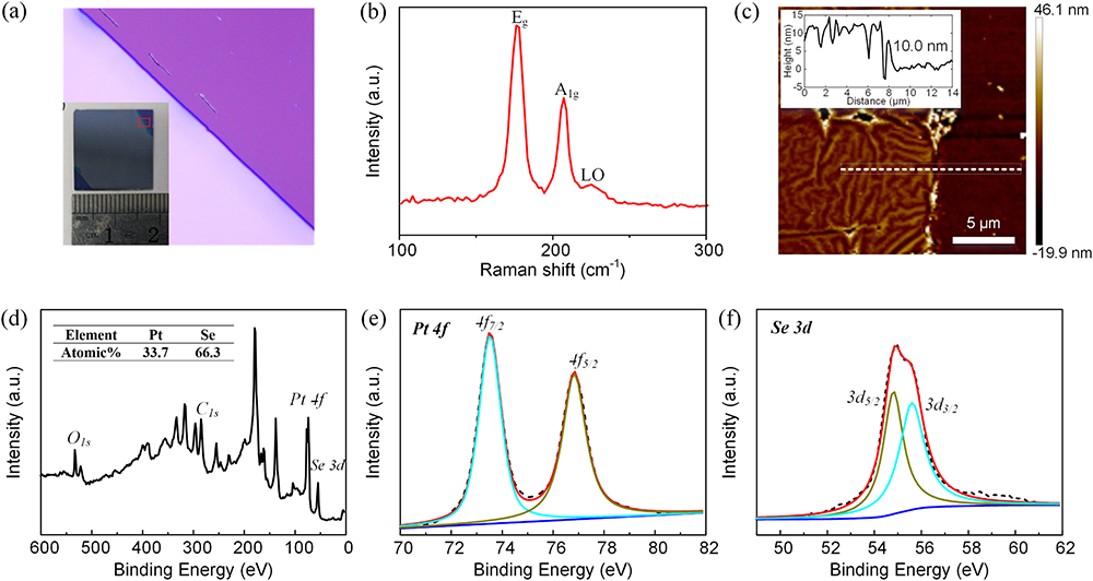
    Fig. 1. (a) Optical microscopy image of the CVD grown PtSe2 film. (b) Raman spectrum of PtSe2 film. (c) AFM image of the transferred PtSe2 and the typical height profile along the white dashed line. XPS spectra of (d) the PtSe2 film, (e) the Pt 4f region, and (f) the Se 3d region.
    (a) Microscope image of the all-optical modulator where PtSe2 film fully covers the whole device. (b) A zoom-in on the part of the MRR shows uniformly transferred thin film. (c) Cross section of the PtSe2-on-silicon structure. (d) Transmission spectra of the MRR without (brown) and with (blue) the PtSe2 film (normalized respectively). (e) All-optical modulation mechanism and experimental setup of the PtSe2-based modulator. TLS, tunable laser source; ASE, amplified spontaneous emission; PC, polarization controller; SMF, single-mode fiber; OSA, optical spectrum analyzer; PD, photodetector; OSCP, oscilloscope.
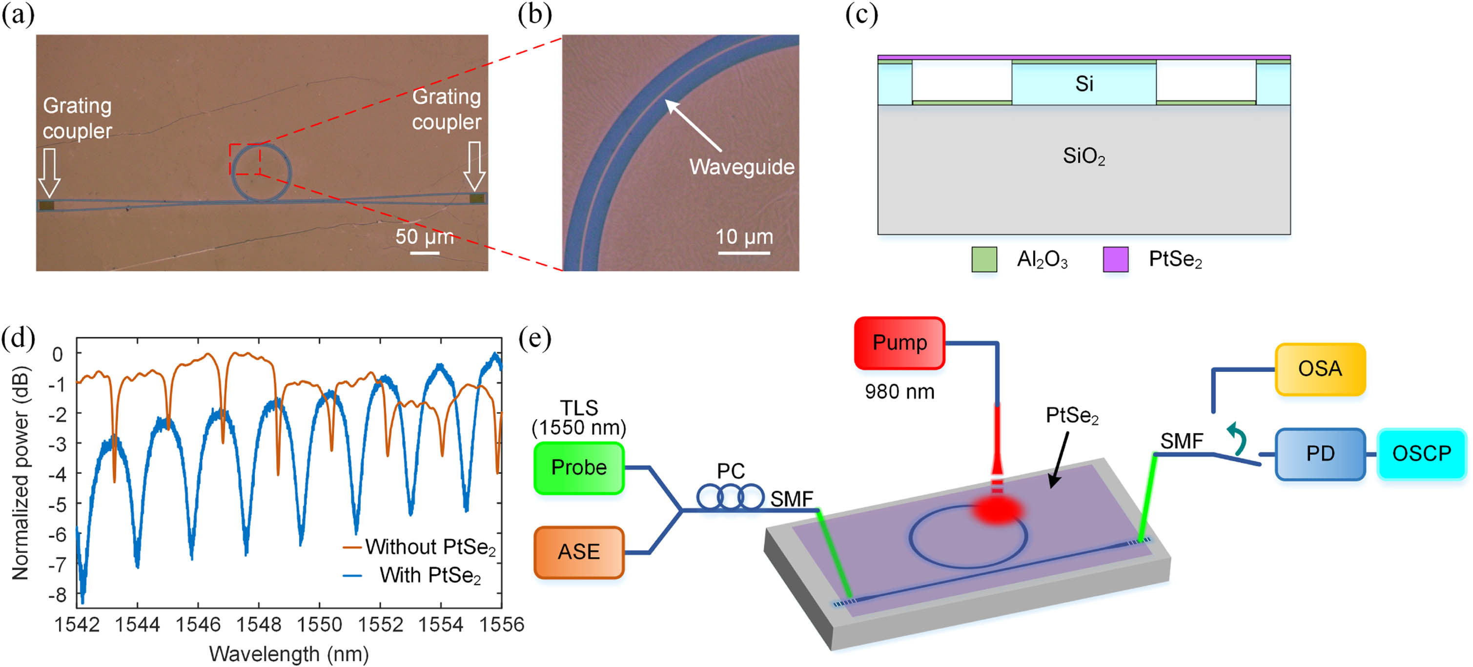
    Fig. 2. (a) Microscope image of the all-optical modulator where PtSe2 film fully covers the whole device. (b) A zoom-in on the part of the MRR shows uniformly transferred thin film. (c) Cross section of the PtSe2-on-silicon structure. (d) Transmission spectra of the MRR without (brown) and with (blue) the PtSe2 film (normalized respectively). (e) All-optical modulation mechanism and experimental setup of the PtSe2-based modulator. TLS, tunable laser source; ASE, amplified spontaneous emission; PC, polarization controller; SMF, single-mode fiber; OSA, optical spectrum analyzer; PD, photodetector; OSCP, oscilloscope.
    (a) Static spectral response for different pump powers. (b) Measured resonance shift versus pump power and the corresponding linear fitting curves, for pristine PtSe2 device (red) and the device after 3-month air exposure (blue).
    Fig. 3. (a) Static spectral response for different pump powers. (b) Measured resonance shift versus pump power and the corresponding linear fitting curves, for pristine PtSe2 device (red) and the device after 3-month air exposure (blue).
    (a) Pump light with 100 Hz frequency and (b) the corresponding modulated signal light. (c) Several signal waveforms at different frequencies. (d) Vpp versus modulation frequency.
    Fig. 4. (a) Pump light with 100 Hz frequency and (b) the corresponding modulated signal light. (c) Several signal waveforms at different frequencies. (d) Vpp versus modulation frequency.
    Infrared thermograms of the PtSe2 modulator with pump powers of (a) 50 mW and (b) 500 mW. (c) Surface temperature change of the modulator versus pump power.
    Fig. 5. Infrared thermograms of the PtSe2 modulator with pump powers of (a) 50 mW and (b) 500 mW. (c) Surface temperature change of the modulator versus pump power.
    (a) Optical microscopy image of the pure silicon MZI. (b) Static spectral response for different pump powers. (c) Measured resonance shift versus pump power and the corresponding fitting curve.
    Fig. 6. (a) Optical microscopy image of the pure silicon MZI. (b) Static spectral response for different pump powers. (c) Measured resonance shift versus pump power and the corresponding fitting curve.
    Pump WavelengthProbe WavelengthInteraction LengthSwitching TimeTuning Efficiency
    MaterialStructure(nm)(nm)(μm)(μs)(nm·mW1)Refs.
    BPSilica fiber980155025000.0043[6]
    WS2Silica fiber980155050073000.0015[7]
    MXeneSilica fiber980155050041000.0086[12]
    AntimoneneSilica fiber98015505029000.0162[53]
    GrapheneSilica fiber980/15401550500032000.0045[11]
    GrapheneSi3N4 waveguide1555150943.40.2530.0079[22]
    PtSe2Silicon waveguide9801550802840.0040This work
    Table 1. Comparison of Reported All-Optical Modulators Based on the Photothermal Effect of 2D Materials
    Kangkang Wei, Delong Li, Zhitao Lin, Zhao Cheng, Yuhan Yao, Jia Guo, Yunzheng Wang, Yupeng Zhang, Jianji Dong, Han Zhang, Xinliang Zhang. All-optical PtSe2 silicon photonic modulator with ultra-high stability[J]. Photonics Research, 2020, 8(7): 1189
    Download Citation