1Wuhan National Laboratory for Optoelectronics, Huazhong University of Science and Technology, Wuhan 430074, China
2Institute of Microscale Optoelectronics, Collaborative Innovation Centre for Optoelectronic Science & Technology, Key Laboratory of Optoelectronic Devices and Systems of Ministry of Education and Guangdong Province, College of Physics and Optoelectronic Engineering, Shenzhen Key Laboratory of Micro-Nano Photonic Information Technology, Guangdong Laboratory of Artificial Intelligence and Digital Economy (SZ), Shenzhen University, Shenzhen 518060, China
All-optical modulation based on the photothermal effect of two-dimensional (2D) materials shows great promise for all-optical signal processing and communication. In this work, an all-optical modulator with a 2D -on-silicon structure based on a microring resonator is proposed and demonstrated utilizing the photothermal effect of . A tuning efficiency of is achieved, and the 10%–90% rise and decay times are 304 μs and 284 μs, respectively. The fabricated device exhibits a long-term air stability of more than 3 months. The experimental results prove that 2D has great potential for optical modulation on a silicon photonic platform.
1. INTRODUCTION
All-optical modulation has received extensive attention since it avoids the conversion of electrical signals to optical signals [1]. Although electrically driven modulators using such as charge carrier injecting effect [2], thermo-optic effect [3], and Pockels effect [4] have achieved great success on silicon and lithium niobate platforms, all-optical modulation still plays an irreplaceable role due to its simple structural design and easy manufacturing process. Meanwhile, novel two-dimensional (2D) materials emerging in recent years, such as graphene [5], black phosphorus (BP) [6], and transition metal dichalcogenides (TMDs) [7], provide more opportunities to implement all-optical signal processing, with respect to their distinct merits, such as intrinsic lattice matching with silicon, complementary metal oxide semiconductor integrability, as well as excellent electrical, optical, and thermal properties [8,9]. Li et al. demonstrate all-optical intensity modulation in a graphene-clad microfiber by using Pauli blocking in graphene; an ultra-fast decay time of 2.2 ps and a modulation depth of 38% are achieved [5]. Thermo-optic effect [10] is also used to achieve all-optical phase modulation in the microfiber assisted by graphene [11], BP [6], MXene [12], or tungsten disulfide () [7], but the response time is of the order of milliseconds. The integrated photonic platform offers higher compactness and potential for manufacturing large-scale photonic integrated circuits [13,14]. All-optical modulation based on an integrated platform has been intensively studied using photo-excited free-carrier concentrations [15], electromagnetic induced transparency [16], reverse saturable absorption [17], or photothermal effect (assisted by metal–insulator–metal absorbers) [18–20], etc. However, 2D material-based all-optical modulation on an integrated photonic platform has been rarely reported [21–24]. It is essential to explore the potential of 2D materials to achieve all-optical modulation on an integrated photonic platform.
As a group of representative 2D materials, TMDs are composed of two chalcogen (X) atomic layers and a transition metal (M) atomic layer sandwiched between them [25]. Compared with the zero bandgap and weak optical absorption (2.3%) of monolayer graphene [26], TMDs have bandgaps that change with the number of layers and strong resonant absorption at specific wavelengths [27]. In addition, TMDs can be prepared by the chemical vapor deposition (CVD) method and other bottom-up growth techniques, which reveal the advantages of excellent uniformity, controllable number of layers, strong reliability, high repeatability, and large area preparation [28,29].
Platinum selenide (), a new type of layered TMD, has been intensively studied due to its special properties since it was first epitaxially grown by direct selenization of Pt on a substrate [30]. Its crystal structure can be regarded as being composed of hexagonal closely arranged Se atoms with Pt atoms occupying octahedral sites in alternate Se layers [25]. Different from other TMDs with large bandgaps (such as monolayer ) [31,32], monolayer has a smaller indirect bandgap of 1.2 eV, while the bilayer directly reduces to 0.21 eV [25,33]. If the thickness continues to increase, it will eventually become a Type II Dirac semimetal without a bandgap [30,34–36], and the absorption of light in a specific band (especially in the range of less than 1000 nm) is even higher than that of an Au film [37]. Previous works have applied 2D to a saturation absorber, photodetector, and field effect transistor, and confirmed that wideband responses can be achieved by changing the number of layers [25,37–45]. In addition, is predicted to have the highest carrier mobility of at room temperature among reported TMDs [46], and a long-term air stability for over 1 year has been reported [47].
Sign up for Photonics Research TOC. Get the latest issue of Photonics Research delivered right to you!Sign up now
In this work, we propose and experimentally demonstrate an all-optical modulator with a 2D -on-silicon structure. The material is grown with the CVD method and then transferred onto a silicon microring resonator (MRR). By using a 980 nm laser to irradiate the surface of the device from free space, we successfully demonstrate all-optical modulation based on the photothermal conversion of PtSe2. A tuning efficiency of is achieved. The dynamic 10%–90% rise/decay time is 304/284 μs, and the 3 dB bandwidth is measured to be 2.4 kHz. We also perform a comparative experiment on a pure silicon device and confirm that the photothermal conversion efficiency almost entirely comes from the 2D . Due to the outstanding air stability of , the tuning efficiency of the fabricated device only decreased by 7.5% after being exposed to the air for 3 months, which exhibits the long-term stability of this all-optical modulator. Results show that the -based device is a potential option to be deployed in all-optical signal processing, showing great advantages in low cost and easy fabrication.
2. DEVICE FABRICATION AND PRINCIPLE
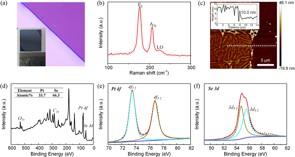
The optical microscopy image of the as-prepared film is illustrated in Fig. 1(a), which indicates that the film is uniform in large size. As shown in Fig. 1(b), three pronounced Raman peaks can be found at , , and , corresponding to the Eg, A1g, and LO vibrational modes of Se atoms, respectively. The positions of these Raman peaks are well consistent with the previously reported values [48,49], which confirms the quality of the as-grown film. The thickness and surface topography of the transferred are characterized by an atomic force microscope (AFM). As shown in Fig. 1(c), the film thickness is determined to be 10.0 nm. However, there are many folds as transferred to the surface of the chip, so the actual thickness of film will be slightly smaller, and the number of layers is about 13 [33]. The species and chemical states of the elements in the film are analyzed by X-ray photoelectron spectroscopy (XPS). According to the XPS analysis, the film has predominant C, O, Pt, and Se peaks shown in Fig. 1(d). However, the peaks of C1s and O1s originate from the absorbed air in the surface of the film. As shown in Figs. 1(e) and 1(f), the Pt 4f and Se 3d spectra of are fitted considering two peaks by Gaussian fitting. According to the fitting spectra, there are two peaks at 73.52 eV and 76.83 eV that are related to Pt 4f7/2 and Pt 4f5/2 orbitals, respectively. Moreover, the peaks located at 54.81 eV and 55.59 eV are related to Se 3d5/2 and Se 3d3/2. The atomic ratios of Pt and Se calculated on the basis of XPS spectra are shown in the inset of Fig. 1(d), which is quite consistent with the theoretical value.
Figure 1.(a) Optical microscopy image of the CVD grown film. (b) Raman spectrum of film. (c) AFM image of the transferred and the typical height profile along the white dashed line. XPS spectra of (d) the film, (e) the Pt 4f region, and (f) the Se 3d region.
The microscope images of the all-optical MRR modulator are displayed in Figs. 2(a) and 2(b). Our device is fabricated on a silicon-on-insulator (SOI) wafer with a 220 nm thick silicon layer and a 2 μm thick buried oxide layer, using standard electron beam lithography followed by the inductively couple plasma etching process. The device consists of a ring-shaped waveguide and a side coupled straight waveguide, where the radius of the ring is 50 μm and the gap of the coupling region is 80 nm. The width of the waveguide is 550 nm and the height is 220 nm. There is a pair of tapered grating couplers at both ends of the straight waveguide for optical coupling between the fiber and the chip. A 10 nm thick isolation layer is deposited onto the SOI wafer using the atomic layer deposition method, as shown in Fig. 2(c). Finally, the thin film is transferred to the device surface by the wet-transfer process.
Figure 2.(a) Microscope image of the all-optical modulator where film fully covers the whole device. (b) A zoom-in on the part of the MRR shows uniformly transferred thin film. (c) Cross section of the -on-silicon structure. (d) Transmission spectra of the MRR without (brown) and with (blue) the film (normalized respectively). (e) All-optical modulation mechanism and experimental setup of the -based modulator. TLS, tunable laser source; ASE, amplified spontaneous emission; PC, polarization controller; SMF, single-mode fiber; OSA, optical spectrum analyzer; PD, photodetector; OSCP, oscilloscope.
Figure 2(d) shows the transmission spectra of the MRR with and without 2D film. The MRR initially operates at the over coupling condition with an extinction ratio (ER) of 3–4 dB and a free spectral range (FSR) of . As the waveguide is coated by film, the round-trip loss of the MRR increases due to the light absorption and the edge scattering effect, while the coupling coefficient between the straight waveguide and the ring may also have changed [50]. Thus, the device works closer to the critical coupling condition with an ER of 5–6 dB. Moreover, the effective refractive index of the grating couplers changes and the peak wavelength moves to a longer wavelength once they were covered by the 2D film. In fact, the extra loss caused by the transferred material is by comparing the transmittance before and after transferring material, including the optical absorption of the material and the deterioration on the grating couplers.
The resonance wavelength of the MRR is given by Eq. (1): where is the effective refractive index of the hybrid waveguide at a specific wavelength, isthe radius of the MRR, and is the resonance order of corresponding wavelength . As shown in Fig. 2(e), the film will absorb the pump light and heat the waveguide underneath due to the photothermal effect. The increase in temperature causes the effective refractive index to change, which performs a redshift in the output spectrum. When the probe light (signal light) of a specific wavelength is injected into the waveguide, the output optical power is (in dB). After being heated by the pump light, the corresponding output power changes to (in dB). Therefore, the output light intensity is modulated by the pump light with a modulation depth (MD) of .
3. EXPERIMENTAL SETUP
The experimental setup of the proposed all-optical modulator is schematically shown in Fig. 2(e). An amplified spontaneous emission (ASE, ALS-18-B-FA, Amonics) light and a tunable laser source (TLS) as a probe light are combined by a 3 dB fiber coupler and then injected into the chip through a single-mode fiber (SMF) and a grating coupler. The polarization of the light beam is controlled by the polarization controller to obtain the quasi-transverse electric mode transmitting in the designed waveguide, which limits the optical field of the probe light to the center of the waveguide to reduce optical loss. Then the output light is coupled into the SMF by another identical grating coupler. Pump light [produced by a home-made programmable 980 nm laser source, which can work in the continuous-wave (CW) mode or square-wave (SW) mode] directly irradiates the device surface through an SMF. Only ASE is turned on at the input end when the pump laser works in the CW mode, and the output SMF is connected to an optical spectrum analyzer (AQ6370D, Yokogawa) to monitor the transmission spectrum of the MRR. Only the TLS is turned on when the pump laser works in the SW mode, and the output SMF switches to the photodetector (DET08CFC/M InGaAs Biased Detector, Thorlabs) and oscilloscope (MDO4104C, Tektronix) path to obtain the dynamic modulation response. All the experiments were carried out at room temperature.
4. RESULTS AND DISCUSSION
A. Experimental Results
The static pump results are shown in Fig. 3. The FSR of the MRR is given by Eq. (2): where is the center wavelength, and is the group index of the waveguide. In order to obtain the maximum MD, the spectral shift produced by the pump light should be larger than half of the full width of the resonance peak. However, the value of the device decreases after the film is transferred, as shown in Fig. 2(d), so the spectral shift must be larger than half of the FSR.
Figure 3.(a) Static spectral response for different pump powers. (b) Measured resonance shift versus pump power and the corresponding linear fitting curves, for pristine device (red) and the device after 3-month air exposure (blue).
The pump power from 0 to 210.9 mW (measured by a hand-held power meter, FPM-300 Power Meter, EXFO) is applied to measure the static response of the device when a 980 nm laser source works in the CW mode. The results in Fig. 3(a) indicate that a phase modulation is obtained in the -based modulator. Once the pump power is reduced, the spectrum will move back to its initial position. The maximum spectral shift is 0.962 nm (i.e., ), and the calculated tuning efficiency is or [red line in Fig. 3(b)]. Compared to the pure silicon device with a tuning efficiency of or (see static spectral response of the pure silicon device in Appendix A), the heating efficiency improvement mainly comes from the film. In order to investigate the stability of the modulator, the static response of the device was tested again after 3 months of exposure to air. As shown in Fig. 3(b) (blue line), a spectral shift of 1.156 nm (i.e., ) is obtained when the maximum pump power is set to be 300 mW, and the tuning efficiency is , which is almost maintained the same as that of the newly fabricated device. These results prove that the all-optical modulator based on 2D has a long-term air stability.
To characterize the dynamic response of the device, the 980 nm pump laser operates in the 100 Hz SW mode with a power of 210 mW [Fig. 4(a)], and the wavelength of the TLS is selected as 1550.3 nm. The corresponding probe light waveform is shown in Fig. 4(b), and the 10%–90% rise and decay times are measured to be 304 μs and 284 μs, respectively. This is 1 order of magnitude faster than that of graphene- and BP-based all-optical modulators using the photothermal effect with a microfiber structure [6,11]. The frequency response of the modulator is further studied by a faster SW signal with the frequency varying from 200 Hz to 10 kHz. Several measured waveforms of the modulated probe light with different frequencies are shown in Fig. 4(c). As the frequency increases, the modulated signal waveform gradually deforms from square wave to triangle wave, and the peak-to-peak voltage (Vpp) of the signal keeps decreasing as the frequency increases, which is mainly attributed to the hysteresis effect of slow heat generation and dissipation [6]. The tendency of Vpp versus modulation frequency is shown in Fig. 4(d), and the fitted 3 dB bandwidth of the device is 2.4 kHz, which is close to the measured rise/decay time.
Figure 4.(a) Pump light with 100 Hz frequency and (b) the corresponding modulated signal light. (c) Several signal waveforms at different frequencies. (d) Vpp versus modulation frequency.
In order to evaluate the true photothermal efficiency of the , the photothermal conversion efficiency of the modulator is calculated by combining the thermo-optic and thermal expansion theory of silicon with Eq. (1). With the increase of temperature, the effective refractive index and length of the waveguide in the region of the pump light irradiation (spot size μ) will change because of the thermo-optic and thermal expansion effects of silicon [51], as shown in Eqs. (3) and (4): where is the thermo-optic coefficient [52] and is the thermal expansion coefficient [51] of silicon, and is the temperature before heating. For an MRR, the spectral shift of the m-order resonant wavelength after heating can be obtained by substituting Eqs. (3) and (4) into Eq. (1): It can be calculated that the desired temperature change to obtain 1 nm resonance shift around 1550 nm is according to Eq. (5), and the refractive index change of the specific waveguide region is . In fact, the thermal expansion coefficient is 2 orders of magnitude smaller than the thermo-optic coefficient, and its effect is almost negligible. As shown in Fig. 3(b), the pump power corresponding to a spectral shift of 1 nm in the static test is . An infrared thermal camera is used to characterize the surface temperature change of the fabricated modulator under different pump power in real time, as shown in Figs. 5(a) and 5(b). The maximum pump power is up to 500 mW in test, and the surface temperature change is with a fitted temperature-power coefficient of 0.0036 K · mW−1, as shown in Fig. 5(c). Therefore, when the 250 mW pump light heats the device, it will cause a temperature change of . This is smaller than our theoretical value, and the reason lies in that the 980 nm pulsed laser is used in the surface temperature test. Its pump energy is lower than that of the CW laser, and the SMF moves far from the modulator due to the restraints of test equipment, thus resulting in a larger light spot and less energy per unit area. At the same time, the heat is more likely to diffuse to areas outside the MRR.
Figure 5.Infrared thermograms of the modulator with pump powers of (a) 50 mW and (b) 500 mW. (c) Surface temperature change of the modulator versus pump power.
Figure 6.(a) Optical microscopy image of the pure silicon MZI. (b) Static spectral response for different pump powers. (c) Measured resonance shift versus pump power and the corresponding fitting curve.
Here a comparison of the reported all-optical modulators based on the photothermal effect of 2D materials is summarized in Table 1. The on-chip waveguide modulators obviously have better compactness and faster modulation speed compared with the modulators using the microfiber structure. In addition, compared with the weak light absorption of graphene on waveguide [22], the greater light absorption of means a lower pump power consumption can be achieved theoretically. Although both schemes achieve the same level of tuning efficiency with interaction lengths μ, considering that when the pump light is irradiated from free space, the width of the waveguide (550 nm) is much smaller than the diameter of the light spot (μ). This means that more than 80% of the energy in the spot cannot be used to effectively heat the microring waveguide (assuming that the energy distribution of the pump spot is similar to the fundamental mode in the SMF). It can be expected that the -based device can achieve better tuning efficiency with optimized pumping methods.
Pump Wavelength
Probe Wavelength
Interaction Length
Switching Time
Tuning Efficiency
Material
Structure
(nm)
(nm)
(μm)
(μs)
(nm·mW−1)
Refs.
BP
Silica fiber
980
1550
—
2500
0.0043
[6]
WS2
Silica fiber
980
1550
500
7300
0.0015
[7]
MXene
Silica fiber
980
1550
500
4100
0.0086
[12]
Antimonene
Silica fiber
980
1550
50
2900
0.0162
[53]
Graphene
Silica fiber
980/1540
1550
5000
3200
0.0045
[11]
Graphene
Si3N4 waveguide
1555
1509
43.4
0.253
0.0079
[22]
PtSe2
Silicon waveguide
980
1550
∼80
284
0.0040
This work
Table 1. Comparison of Reported All-Optical Modulators Based on the Photothermal Effect of 2D Materials
Therefore, it is possible to achieve more efficient pumping by using a lensed fiber tip to reduce the size of the spot [20]. The silicon-based thermo-optic modulator has achieved a response time of 0.6 μs [3], which means accurate material etching and specific optimized air gaps that can help the heat distribution to be concentrated on the waveguide rather than spread far away [20], which may further improve the modulation efficiency and response speed of the device. In addition, the demanded spectral shift and the corresponding pump power can be reduced by optimizing the factor of the device. The optical losses of the device are mainly attributed to the contamination during the process of material transferring and the absorption caused by the material covering the grating couplers and other non-pumping parts, which can be eliminated by patterning definition [54].
5. CONCLUSION
In conclusion, we propose and demonstrate an all-optical modulator with a -on-silicon structure. By utilizing the photothermal effect of , we successfully convert the information from pump light to probe light. The device achieves a modulation bandwidth of 2.4 kHz with a 10%–90% rise/decay time of 304/284 μs, and the tuning efficiency is . Thanks to the long-term stability of in the air, the tuning efficiency of the device keeps almost unchanged after 3 months. This work brings 2D to the field of silicon-based photothermal modulation devices for the first time and shows its great potential for the all-optical information processing field, such as optical routing, switching, and logic gate and sensing, with low cost and simple manufacturing process.
Acknowledgment
Acknowledgment. The authors also acknowledge the support from Instrumental Analysis Center of Shenzhen University (Xili Campus).
APPENDIX A
Synthesis of the <inline-formula><math display="inline" id="m94" xmlns:mml="http://www.w3.org/1998/Math/MathML"><mrow><msub><mrow><mi>PtSe</mi></mrow><mrow><mn>2</mn></mrow></msub></mrow></math></inline-formula> Film
The in this work was grown by a simple selenization method. In brief, 5?nm Pt film was first deposited on (300?nm thickness) using a magnetron sputtering system. The metal-deposited substrates were placed at the center zone of the growth furnace and elemental selenium powder (99.99% purity) was placed at the upstream side. Selenium was evaporated at 220°C dragged by 50 SCCM (standard cubic centimeter per minute) argon flow. The center temperature of the tube furnace was set to be 420°C. After selenization for 1?h, a thin film will be formed at the substrate.
Wet-Transfer Process
The films were spin-coated with 5% (mass fraction) polymethylmethacrylate (PMMA) in chlorobenzene, and then the underlying was removed in NaOH solution. The film was rinsed in de-ionized water to remove the remaining ions. Afterward, the silicon chip was soaked in de-ionized water solution, and then slowly lifted to transfer the films on the SOI chip surface. Then, the PMMA was dissolved in acetone.
Static Spectral Response of the Pure Silicon Device
As shown in Fig.?6, we used a silicon Mach–Zehnder interferometer (MZI) that was fabricated on the same silicon wafer without transferring the 2D film to perform the photothermal modulation of the pure silicon device, where the parameters of the waveguide are exactly the same as those in the MRR. The difference between the two arms is ~μ, which corresponds to an FSR of ~ around 1550?nm. When a 980?nm CW laser directly illuminated one arm of the MZI with pump power ranging from 0 to 300?mW, the static spectral response and tuning efficiency of the pure silicon device were obtained.
[24] H. Wang, N. Yang, L. Chang, C. Zhou, S. Li, M. Deng, Z. Li, Q. Liu, C. Zhang, Z. Li, Y. Wang. CMOS-compatible all-optical modulator based on the saturable absorption of graphene. Photon. Res., 8, 468-474(2020).
[45] K. Zhang, M. Feng, Y. Ren, F. Liu, X. Chen, J. Yang, X. Yan, F. Song, J. Tian. Q-switched and mode-locked Er-doped fiber laser using PtSe2 as a saturable absorber. Photon. Res., 6, 893-899(2018).