Abstract
Using a strong nonlinear saturation absorption effect is one technique for breaking through the diffraction limit. In this technique, formation of a dynamic and reversible optical pinhole channel and transient superresolution is critical. In this work, a pump–probe transient detection and observation–experimental setup is constructed to explore the formation process directly. A Ge2Sb2Te5 thin film with strong nonlinear saturation absorption is investigated. The dynamic evolution of the optical pinhole channel is detected and imaged, and the transient superresolution spot is directly captured experimentally. Results verify that the superresolution effect originates from the generation of an optical pinhole channel and that the formation of the optical pinhole channel is dynamic and reversible. A good method is provided for direct detection and observation of the transient process of the superresolution effect of nonlinear thin films.1. INTRODUCTION
A nanoscale spot is very useful for nano-data storage, superresolved light imaging, and nanolithography. However, achieving a nanoscale spot using a lens-based light system is difficult because of the diffraction limit effect. One technique for breaking through the diffraction limits is the optical nonlinear effect, which is referred to as nonlinear superresolution [1–4]. One of the methods of nonlinear superresolution is using the intensity-dependent nonlinear saturation absorption (NSA) effect [5–7].
A collimated Gaussian laser beam is focused on an NSA thin film. The focused spot induces the NSA effect. In NSA, the higher the light intensity, the larger the transmittance. Thus, the largest transmittance is found at the central region of the focused spot and gradually decreases along the radial direction from this spot, thereby inducing a below-diffraction-limited optical pinhole channel. Figure 1 shows a basic schematic of the physical concept of the nonlinear superresolution effect; here a focused beam passes through an optical pinhole channel, and a superresolution spot can be generated at the bottom of the NSA thin film. Nanoscale data storage, lithography, and imaging can be achieved by the interaction of the superresolution spot with the sample through near-field coupling.
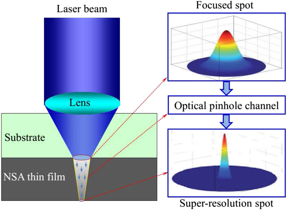
Figure 1.Schematic of the NSA-induced superresolution spot effect.
In NSA-induced superresolution, the NSA thin films must feature large linear and nonlinear absorption coefficients as well as fast time responses. A key consideration is that the formation of an optical pinhole channel is transient and reversible; these features can generate transient and reversible superresolution spots [8–11]. That is, when the laser pulse is switched on, the optical pinhole channel is open. The optical pinhole channel can be automatically closed when the laser pulse is switched off, and the NSA thin film returns to its initial state. The formation of a superresolution spot is thus dynamic and reversible. We have noted that Waldecker et al. found that the decoupled optical response and structural transition in phase change materials are on the scale of femtosecond/picoseconds for typical phase change material [12]. However, in the superresolution effect of phase change materials, the laser pulse is on the scale of nanoseconds, and thus the formation of the superresolution effect on the scale of nanoseconds is more interesting and significant.
Sign up for Photonics Research TOC. Get the latest issue of Photonics Research delivered right to you!Sign up now
In most experiments, the superresolution spots are observed by near-field optical probe scanning experiments statically [13–18]. However, to understand the NSA-induced superresolution further, the transient and reversible optical pinhole channel and superresolution spot must be directly observed and imaged dynamically.
In this work, we construct an experimental setup and explore the dynamic reversible characteristics of an optical pinhole channel. We also directly observe the transient superresolution spot, and the transient superresolution effect is analyzed and discussed. This paper is organized as follows. Section 2 gives the experiment description. Section 3 presents the experimental results and analysis, and Section 4 provides the conclusion.
2. EXPERIMENT DESCRIPTION
Figure 2 illustrates the setup, where a typical pump–probe technique is used. The setup is also very similar to the static tester systems in the phase change research field [19–21]. A GaN semiconductor blue-violet laser (BVL) diode (marked as 2 in Fig. 2), which emits a laser beam of 405 nm wavelength, is connected to one of the two channels of a signal generator (marked as 1). The BVL is modulated into an arbitrary light pulse by the signal generator, and the shortest pulse width is 20 ns. The BVL is used as a pump laser. The pump laser is divided into two parts by a splitter with a splitting ratio of (marked as 3). One part of the pump laser is focused to a high-speed photoelectronic detector (HPD) (marked as 5) and used to monitor the pump pulse waveform. The other part of the pump pulse passes through a 1/2 wave plate (WP) (marked as 6) and becomes -polarized light. The -polarized light ordinally passes through the polarized beam splitter (PBS) (marked as 7) and the 1/4 WP (marked as 8) and becomes circularly polarized light. The circularly polarized light is reflected into a beam expander (marked as 14) by a dielectric mirror (marked as 13), reflected into an objective lens (OL), and focused onto a pump spot on the sample surface (marked as 18). The pump spot induces the optical nonlinear effect and generates an optical pinhole channel inside the sample. The reflected pump light from the sample again passes through the 1/4 WP (marked as 8) and becomes -polarized light. The -polarized pump light is insulated from the BVL device, which can prevent the reflected light from entering the laser diode and producing ill effects on the stability of the pump light.

Figure 2.Experimental setup. 1, signal generator; 2, BVL; 3, splitter (); 4, lens; 5, HPD; 6, 1/2 WP for BVL; 7, PBS for BVL; 8, 1/4 WP for BVL; 9, RL laser; 10, 1/2 WP for RL; 11, PBS for RL; 12, 1/4 WP for RL; 13, dichroic beam splitter; 14, beam expander; 15, reflector; 16, OL for focusing; 17, sample stage; 18, sample; 19, OL for collecting signal; 20, filter for RL; 21, splitter (); 22, lens; 23, HPD; 24, lens; 25, ICCD; 26, lens; 27, HPD.
Another semiconductor red laser (RL) diode emits a continuous light beam with a wavelength of 685 nm and is used as a probe light to explore the transient and reversible characteristics of the optical pinhole channel and superresolution spot. The probe light passes through a 1/2 WP (marked as 10) and becomes -polarized light. The -polarized light ordinally passes through the PBS (marked as 11) and 1/4 WP (marked as 12) and becomes circularly polarized probe light. The circularly polarized probe light passes through the dielectric mirror (marked as 13) and enters the beam expander (marked as 14), where the probe and pump lights are coaxially combined into a beam by the dielectric mirror. The expanded probe light beam is reflected into the OL (marked as 16) for focusing by the reflector (marked as 15). The OL focuses the probe light onto the sample surface, and the focused probe light spot overlaps the pump light spot.
The pump spot induces the nonlinear effect and leads to the formation of the optical pinhole channel; the low-power probe light passes through the optical pinhole channel, and the superresolution spot is generated on the exiting surface of the sample. The superresolution spot signal is collected by an OL with a high numerical aperture (NA) (marked as 19). The collected superresolution spot signal passes through a filter (marked as 20), where the pump light is filtered out and only the probe light signal passes through the filter. The collected probe light is divided into two parts by a splitter (marked as 21) with a splitting ratio of 5:5. One part is focused onto an HPD (marked as 23), and the other is focused onto an intensified CCD (ICCD) (Andor iSRAT, marked as 25) to image and observe the superresolution spot directly. One of the two channels of the signal generator is connected to the ICCD to trigger its shutter. The ICCD has a minimum gate width of 2 ns. The delay time between the pump pulse and the ICCD shutter trigger can be arbitrarily tuned by the signal generator.
The reflected probe light from the sample again passes through the 1/4 WP (marked as 12) and becomes -polarized probe light. The -polarized probe light is then incident on the PBS (marked as 11) and reflected at 90° and focused onto the HPD (marked as 27).
Here the thin film is taken as an example because of its strong NSA characteristics [22–25]. The nonlinear characteristics can be directly obtained by the semiconductor-laser-diode-based z-scan method due to the strong linear absorption in visible light [26]. The sample structure is called “,” where is used to prevent the thin film from being oxidized and damaged.
3. EXPERIMENTAL RESULTS AND ANALYSIS
The dynamic and reversible characteristics of the optical pinhole channel can be analyzed through the transmitted probe light signal obtained from the HPD (marked as 23 in Fig. 2). Figure 3 provides a set of typical experimental results. The pump pulse width is set to 50 ns, and the laser power is 34 mW. The probe light signals reflected from the optical pinhole channel are also shown in Fig. 3.
Figure 3.Reversible characteristics of the optical pinhole channel.
In Fig. 3, pump pulses with a width of 50 ns are irradiated onto the thin film, and the intensity of every pump pulse remains unchanged. Every pump pulse induces the formation of an optical pinhole channel only once. Each pump pulse corresponds to a transmitted probe light signal and a reflected probe light signal. The transmitted and reflected probe light signals present evident peak and valley characteristics, respectively, which indicate that the optical pinhole channel is generated when the pump pulse interacts with the thin film. When the pump pulse is switched off, the transmitted and reflected probe light signals return to their initial states. When another pump pulse reaches the thin film, the optical pinhole channel is formed once more, and the transmitted and reflected probe light signals again present evident peak and valley characteristics, respectively. The optical pinhole channel can be formed many times and presents dynamic and reversible characteristics.
To understand the formation dynamics of an optical pinhole channel further, the time response of an optical pinhole channel induced by a single pump pulse is analyzed. Figure 4 demonstrates typical experimental results obtained with a pump pulse full width of 80 ns and laser power of 20 mW; here, both the reflected and transmitted probe light signals are presented. The reflected and transmitted probe light signals begin to change simultaneously after the peak value of the pump pulse; that is, the response of the thin film to the pump pulse lags for 20 ns, which may be attributed to the nonlinear effect of , partially resulting from the thermal effect. The nonlinear effect only occurs when the temperature exceeds a certain threshold. This finding reflects the presence of a threshold for the formation of an optical pinhole channel. After this threshold, the transmitted and reflected probe light signals quickly increase from their initial values at the peak of the pump pulse to their maximum values at the end of the pump pulse, and an optical pinhole channel thoroughly forms accordingly. This phenomenon suggests that the optical pinhole channel completely opens at this time and reveals that the opening time is approximately 20 ns. After the pump pulse, the optical pinhole channel gradually closes and the transmitted and reflected probe light signals return to their initial states. The closing time is around 120 ns, which is longer than the opening time of 20 ns. The closing of the optical pinhole channel may result from the thermal structural relaxation; thus, the closing time of the optical pinhole channel is longer than its opening time.
Figure 4.Time response of a single pump-pulse-induced optical pinhole channel (pump pulse width of 80 ns, power of 20 mW).
The dynamic formation process of an optical pinhole channel is also directly observed in the transient spot images, as shown in Fig. 5, where the transient spots are obtained by the ICCD imaging at different delay times. In this experiment the high-NA lens (marked as 24) before the ICCD is selected to obtain a small focused spot in the ICCD and improve the contrast of the light intensity among spot images at different delay times. Thus, the transient spot images contain several pixels only. This characteristic does not negatively affect the experimental analysis of the dynamic formation process of an optical pinhole channel. Every transient spot image is captured at a shutter gate width of 10 ns.
Figure 5.Transmitted transient probe spots at delay times of (a) 0, (b) 60, (c) 80, (d) 120, and (e) 200 ns, respectively corresponding to letters A, B, C, D, and E in Fig. 4.
Figure 5(a) shows the probe spot image obtained at zero delay time, which corresponds to letter A in Fig. 4. The optical pinhole channel is not formed at this time, and the brightness (or intensity) of the probe spot is very low. Figure 5(b) shows the probe spot image obtained at 60 ns delay time, which corresponds to B in Fig. 4. The probe spot is fairly obvious and bright compared with that at zero delay time, and the central intensity reaches approximately 120% of the central intensity of the initial spot. These results indicate formation of the optical pinhole channel. The optical pinhole channel thoroughly opens at a delay time of 80 ns, which corresponds to C in Fig. 4; this probe spot is shown in Fig. 5(c). At a delay time of 80 ns the probe spot is the strongest and brightest and the central intensity reaches approximately 150% of the central intensity of initial spot. This result indicates that the optical pinhole channel has formed and is completely open at this time. The delay time of 80 ns actually corresponds to the end of pump pulse. Hence, the optical pinhole channel thoroughly opens at the end of the pump pulse, and the transmitted probe spot intensity is the largest at this time point compared with those in Figs. 5(a) and 5(b).
After the pump pulse, the optical pinhole channel begins to close, and the close time is approximately 120 ns, as can be seen from the transmitted probe light signal in Fig. 4. The transmitted probe spot weakens with increasing delay time. In Fig. 5(d), the transient transmitted probe spot is obtained at a delay time of 120 ns; that is, the spot image is captured at 40 ns after the pump pulse, which corresponds to D in Fig. 4. The central intensity is about 130% of the central intensity of initial spot. The intensity is weaker than that in Fig. 5(c), which is due to the fact that the optical pinhole channel has decreased in size and the transmittance has decreased accordingly. Increases in delay time further decrease the optical pinhole channel transmittance. The spot image is captured at a delay time of 200 ns, which corresponds to E in Fig. 4. The transmitted probe spot is presented in Fig. 5(e); here the central intensity is similar to that of the initial probe spot in Fig. 5(a). This result indicates that the optical pinhole channel has thoroughly closed, and the thin film returns to its initial state. The combination of Figs. 4 and 5 experimentally verifies that the formation of an optical pinhole channel is dynamic and reversible.
After formation of an optical pinhole channel, the probe light travels through the optical pinhole channel and a superresolution probe spot is produced at the exiting surface of the sample. Generation of the superresolution probe spot is also transient and reversible. The transient superresolution spot can be directly imaged by the ICCD (marked as 25 in Fig. 2). This experiment is different from those illustrated in Figs. 4 and 5. To capture spot images occupying more pixels, a low-NA lens (marked as 24 in the experimental setup) before the ICCD is used to replace the high-NA lens installed before the ICCD of Figs. 4 and 5.
Figure 6 illustrates typical transient spot results; here, the pump pulse full width and power are 80 ns and 20 mW, respectively. The shutter gate width is set to 10 ns. The trigger time of the ICCD is delayed for 80 ns after the pump pulse. Figure 6(a) shows an initial transient spot without the pump pulse excitation. Figure 6(b) shows a transient superresolution spot captured at a delay time of 80 ns after pump pulse excitation. The central light intensity of the transient superresolution spot in Fig. 6(b) is larger than that in Fig. 6(a), which indicates that the optical pinhole channel is transiently produced. The probe light passes through the optical pinhole channel, and a bright superresolution spot occurs transiently. Reductions in the transient superresolution spot size can be clearly seen in Fig. 6(c), where the normalized intensity profiles of Figs. 6(a) and 6(b) are compared. The red and blue curves are the Gaussian fittings from the experimental data in Figs. 6(a) and 6(b) marked in yellow. The red curve corresponds to the initial spot without pump pulse excitation, and the blue curve corresponds to the transient superresolution spot with pump pulse excitation. The size of the transient superresolution spot is reduced compared with the initial spot, and the reduction ratio is about 75%. These experimental results further verify that the transient superresolution spot can be formed when the probe light passes through the optical pinhole channel, which is produced by pump pulse excitation.
Figure 6.Transient superresolution probe spot. (a) The initial transient spot without the pump pulse excitation, (b) the transient superresolution spot captured at a delay time of 40 ns after the pump pulse excitation, (c) the comparison of the normalized intensity profiles of (a) and (b).
4. SUMMARY
In summary, the present experimental setup, exploring the dynamic and reversible characteristics of an optical pinhole channel and observing the transient superresolution spot, is constructed. The thin film is used as the NSA thin film. The dynamic and reversible characteristics of the transient optical pinhole channel are demonstrated experimentally. The evolution of the optical pinhole channel is detected and imaged, and the transient superresolution spot is directly obtained by ICCD imaging. The experimental results further verify that for NSA thin films irradiated by a focused Gaussian laser beam, formation of the optical pinhole channel and the transient superresolution spot is dynamic and reversible. This study provides a method for direct detection and observation of the transient evolution of the superresolution effect of nonlinear thin films.
References
[1] J. Wei. Nonlinear Super-resolution Nano-Optics and Applications(2015).
[2] R. Wang, J. Wei. Parabolic approximation analytical model of super-resolution spot generation using nonlinear thin films: theory and simulation. Opt. Commun., 316, 220-227(2014).
[3] C. Barsi, J. W. Fleischer. Nonlinear Abbe theory. Nat. Photonics, 7, 639-643(2013).
[4] L. E. Helseth. Breaking the diffraction limit in nonlinear materials. Opt. Commun., 256, 435-438(2005).
[5] S. Tofighi, A. R. Bahrampour. Theoretical model for visible light saturable absorber nanolithography. J. Opt., 14, 125004(2012).
[6] J. Wei, H. Yan. Strong nonlinear saturation absorption-induced optical pinhole channel and super-resolution effects: a multi-layer system model. Opt. Lett., 39, 6387-6390(2014).
[7] J. Tominaga, T. Nakano, N. Atoda. An approach for recording and readout beyond the diffraction limit with an Sb thin film. Appl. Phys. Lett., 73, 2078-2080(1998).
[8] R. E. Simpson, P. Fons, X. Wang, A. V. Kolobov, T. Fukaya, J. Tominaga. Non-melting super-resolution near-field apertures in Sb-Te alloys. Appl. Phys. Lett., 97, 161906(2010).
[9] T. Fukaya, J. Tominaga, T. Nakano, N. Atoda. Optical switching property of a light-induced pinhole in antimony thin film. Appl. Phys. Lett., 75, 3114-3116(1999).
[10] F. Zhai, F. Zuo, H. Huang, Y. Wang, T. Lai, Y. Wu, F. Gan. Optical switch formation in antimony super-resolution mask layers induced by picosecond laser pulses. Chin. Phys. Lett., 27, 014209(2010).
[11] D. Tsai, C. W. Yang, W. C. Lin, F. H. Ho, H. J. Huang, M. Y. Chen, T. F. Tseng, C. H. Lee, C. J. Yeh. Dynamic aperture of near-field super resolution structures. Jpn. J. Appl. Phys., 39, 982-983(2000).
[12] L. Waldecker, T. A. Miller, M. Rude, R. Bertoni, J. Osmond, V. Pruneri, R. Simpson, R. Ernstorfer, S. Wall. Decoupled optical response and structural transition in phase change materials.
[13] M. Xiao. Theoretical treatment for scattering scanning near-field optical microscopy. J. Opt. Soc. Am. A, 14, 2977-2984(1997).
[14] J. Wei, J. Liu. Direct observation of below-diffraction-limited optical spot induced by nonlinear saturable absorption of Ag-doped Si nanofilms. Opt. Lett., 35, 3126-3128(2010).
[15] A. Goy, D. Psaltis. Imaging in focusing Kerr media using reverse propagation. Photon. Res., 1, 96-101(2013).
[16] A. C. Assafrao, A. J. H. Wachters, M. Verheijen, A. M. Nugrowati, S. F. Pereira, H. P. Urbach, M. Armand, S. Olivier. Direct measurement of the near-field super resolved focused spot in InSb. Opt. Express, 20, 10426-10437(2012).
[17] B. Song, J. Lee, J. H. Kim, K. Cho, S. K. Kim. Direct observation of self-focusing with subdiffraction limited resolution using near-field scanning optical microscope. Phys. Rev. Lett., 85, 3842-3845(2000).
[18] D. P. Tsai, W. C. Lin. Probing the near fields of the super-resolution near-field optical structure. Appl. Phys. Lett., 77, 1413-1415(2000).
[19] K. Watabe, P. Polynkin, M. Mansuripur. Optical pump and probe test system for thermal characterization of thin metal and phase-change films. Appl. Opt., 44, 3167-3173(2005).
[20] M. Mansuripur, J. K. Erwin, W. Bletscher, P. Khulbe. Static tester for characterization of phase change, dye polymer, and magneto-optical media for optical data storage. Appl. Opt., 38, 7095-7104(1999).
[21] C. B. Peng, M. Mansuripur. Amorphization induced by subnanosecond laser pulses in phase-change optical recording media. Appl. Opt., 43, 4367-4375(2004).
[22] S. Liu, J. Wei, F. Gan. Optical nonlinear absorption characteristics of crystalline Ge2Sb2Te5 thin films. J. Appl. Phys., 110, 033503(2011).
[23] Y. H. Fu, Y. L. Lu, P. H. Chang, W. Hsu, S. Tsai, D. P. Tsai. Z-scan study of nonlinear optical coupling of PtOx and Ge2Sb2Te5 of near-field optical recording structure. Jpn. J. Appl. Phys., 45, 7224-7227(2006).
[24] H. S. Lee, B. Cheong, T. S. Lee, J. Jeong, S. Lee, W. M. Kim, D. Kim. Origin of nonlinear optical characteristics of crystalline Ge-Sb-Te thin films for possible superresolution effects. Jpn. J. Appl. Phys., 46, L277-L279(2007).
[25] H. S. Lee, T. S. Lee, Y. Lee, J. Kim, S. Lee, J. Huh, D. Kim, B. Cheong. Microstructural and optical analysis of superresolution phenomena due to Ge2Sb2Te5 thin films at blue light regime. Appl. Phys. Lett., 93, 221108(2008).
[26] H. Yan, J. Wei. False nonlinear effect in z-scan measurement based on semiconductor laser devices: theory and experiments. Photon. Res., 2, 51-58(2014).


