• Chinese Optics Letters
  • Vol. 20, Issue 2, 022501 (2022)
Chao Ning1、2, Tian Yu1、2, Shuman Liu1、2、*, Jinchuan Zhang1、2, Lijun Wang1、2, Junqi Liu1、2, Ning Zhuo1、2、**, Shenqiang Zhai1、2, Yuan Li1、2, and Fengqi Liu1、2、3
Author Affiliations
  • 1Beijing Key Laboratory of Low Dimensional Semiconductor Materials and Devices, Key Laboratory of Semiconductor Materials Science, Institute of Semiconductors, Chinese Academy of Sciences, Beijing 100083, China
  • 2Center of Materials Science and Opto-Electronic Engineering, University of Chinese Academy of Sciences, Beijing 100049, China
  • 3Beijing Academy of Quantum Information Sciences, Beijing 100193, China
  • show less
    DOI: 10.3788/COL202220.022501 Cite this Article Set citation alerts
    Chao Ning, Tian Yu, Shuman Liu, Jinchuan Zhang, Lijun Wang, Junqi Liu, Ning Zhuo, Shenqiang Zhai, Yuan Li, Fengqi Liu. Interband cascade lasers with short electron injector[J]. Chinese Optics Letters, 2022, 20(2): 022501 Copy Citation Text show less
    Energy band diagram of an ICL active stage i composed of an InAs/Ga0.7In0.3Sb/InAs W-type active QW sandwiched by an InAs/AlSb chirped superlattice electron injector on the left side and a GaSb/AlSb double QW hole injector on the right side. Calculated probability density functions are shown for the upper and lower lasing subbands Ee_i and Eh_i, the hole injection level Ehj_i, and the electron injection miniband, where the lowest electron injection level is Eej_i. Four InAs QWs in the electron injector of stage i + 1 are also shown on the right side to illustrate the SMIF for carrier transfer between two sequent stages. The layer structure of the active stage i from the left is as follows: 2.5 nm AlSb/3.0 nm InAs/1.2 nm AlSb/2.7 nm InAs/1.2 nm AlSb/2.4 nm InAs/1.2 nm AlSb/2.0 nm InAs/1.2 nm AlSb/1.8 nm InAs/1.1 nm AlSb/1.7 nm InAs/2.5 nm AlSb/1.7 nm InAs/3.0 nm Ga0.7In0.3Sb/1.4 nm InAs/1.0 nm AlSb/3.0 nm GaSb/1.0 nm AlSb/4.5 nm GaSb/2.5 nm AlSb. Four underlined InAs electron injector QWs were doped with Si to 2 × 1018 cm-3. The bulk conduction band (CB) edge and valence band (VB) edge are indicated by the dark blue and purple lines, respectively.
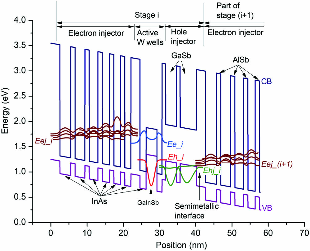
    Fig. 1. Energy band diagram of an ICL active stage i composed of an InAs/Ga0.7In0.3Sb/InAs W-type active QW sandwiched by an InAs/AlSb chirped superlattice electron injector on the left side and a GaSb/AlSb double QW hole injector on the right side. Calculated probability density functions are shown for the upper and lower lasing subbands Ee_i and Eh_i, the hole injection level Ehj_i, and the electron injection miniband, where the lowest electron injection level is Eej_i. Four InAs QWs in the electron injector of stage i + 1 are also shown on the right side to illustrate the SMIF for carrier transfer between two sequent stages. The layer structure of the active stage i from the left is as follows: 2.5 nm AlSb/3.0 nm InAs/1.2 nm AlSb/2.7 nm InAs/1.2 nm AlSb/2.4 nm InAs/1.2 nm AlSb/2.0 nm InAs/1.2 nm AlSb/1.8 nm InAs/1.1 nm AlSb/1.7 nm InAs/2.5 nm AlSb/1.7 nm InAs/3.0 nm Ga0.7In0.3Sb/1.4 nm InAs/1.0 nm AlSb/3.0 nm GaSb/1.0 nm AlSb/4.5 nm GaSb/2.5 nm AlSb. Four underlined InAs electron injector QWs were doped with Si to 2 × 1018 cm-3. The bulk conduction band (CB) edge and valence band (VB) edge are indicated by the dark blue and purple lines, respectively.
    (a) High-resolution XRD pattern measured around GaSb (004) (top) of the epitaxial complete device structure and the dynamic simulation of the same structure (bottom); (b) AFM image measured on the surface of a complete device structure.
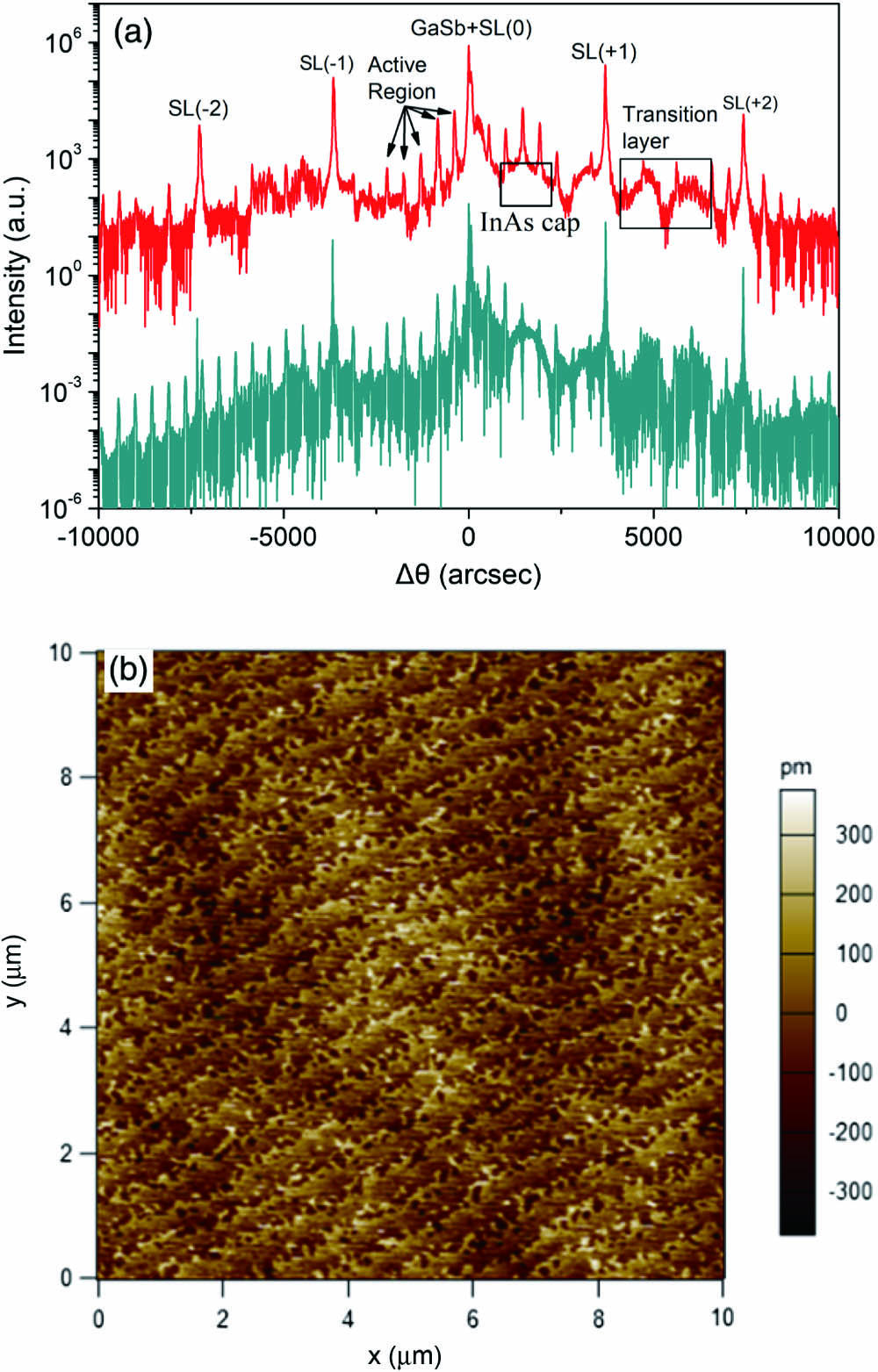
    Fig. 2. (a) High-resolution XRD pattern measured around GaSb (004) (top) of the epitaxial complete device structure and the dynamic simulation of the same structure (bottom); (b) AFM image measured on the surface of a complete device structure.
    Lasing spectra of the ICL at various temperatures.
    Fig. 3. Lasing spectra of the ICL at various temperatures.
    (a) Measured inverse of the external quantum efficiency 1/ηext as a function of cavity length L and (b) threshold current density Jth as a function of the reciprocal of cavity length 1/L. Values of internal quantum efficiency, internal loss, peak modal differential gain, and transparency current density are obtained by fitting the data with Eqs. (1) and (2).
    Fig. 4. (a) Measured inverse of the external quantum efficiency 1/ηext as a function of cavity length L and (b) threshold current density Jth as a function of the reciprocal of cavity length 1/L. Values of internal quantum efficiency, internal loss, peak modal differential gain, and transparency current density are obtained by fitting the data with Eqs. (1) and (2).
    CW L-I-V characteristics for a 15-µm-wide, 5-mm-long device with HR and AR coating at various heat-sink temperatures between 10°C and 60°C.
    Fig. 5. CW L-I-V characteristics for a 15-µm-wide, 5-mm-long device with HR and AR coating at various heat-sink temperatures between 10°C and 60°C.
    (a) CW threshold current densities and (b) differential slope efficiencies versus temperature for an HR/AR and an UN/UN samples.
    Fig. 6. (a) CW threshold current densities and (b) differential slope efficiencies versus temperature for an HR/AR and an UN/UN samples.
    (a) CW output power of a 15 µm × 3 mm ICL. The data were recorded every hour. (b) L-I-V characteristics for the ICL measured before the lifetime test (0 h) and after CW operation for 3500 h, 3900 h, 4700 h, and 6400 h.
    Fig. 7. (a) CW output power of a 15 µm × 3 mm ICL. The data were recorded every hour. (b) L-I-V characteristics for the ICL measured before the lifetime test (0 h) and after CW operation for 3500 h, 3900 h, 4700 h, and 6400 h.
    Chao Ning, Tian Yu, Shuman Liu, Jinchuan Zhang, Lijun Wang, Junqi Liu, Ning Zhuo, Shenqiang Zhai, Yuan Li, Fengqi Liu. Interband cascade lasers with short electron injector[J]. Chinese Optics Letters, 2022, 20(2): 022501
    Download Citation