
Chao Ning, Tian Yu, Shuman Liu, Jinchuan Zhang, Lijun Wang, Junqi Liu, Ning Zhuo, Shenqiang Zhai, Yuan Li, Fengqi Liu, "Interband cascade lasers with short electron injector," Chin. Opt. Lett. 20, 022501 (2022)
- Chinese Optics Letters
- Vol. 20, Issue 2, 022501 (2022)
Abstract
1. Introduction
The interband cascade laser (ICL)[
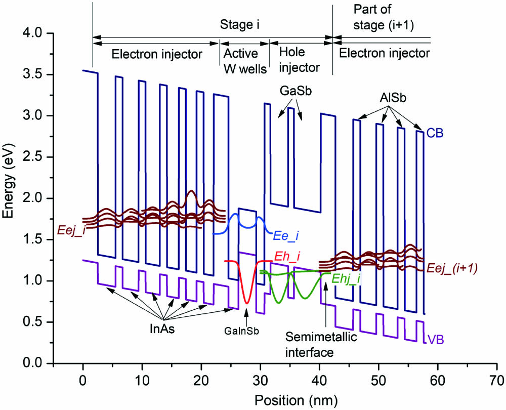
In a well-known quantum cascade laser, only electrons contribute to the current flow by passing through the conduction subbands in each cascade stage. In contrast, both electrons and holes are injected into the active W wells by the electron injector and hole injector on both sides, as shown in Fig. 1. Under an appropriate applied bias voltage, a semi-metallic interface (SMIF) forms between the hole injector and the electron injector due to the type II heterojunction between InAs and GaSb. Such an SMIF is essential to ensure the smooth transport of the electrons between stages. If one pays attention to low power consumption, the SMIF should form under a bias voltage as low as possible. The InAs QW on the right side of the SMIF should be thick enough to lower the ground energy level. This electron energy level is lower than the upper lasing energy level in the next stage. Thus, the electron injection is inefficient in earlier ICLs. On the contrary, holes are generated internally from the intrinsically
![]()
Figure 1.Energy band diagram of an ICL active stage i composed of an InAs/Ga0.7In0.3Sb/InAs W-type active QW sandwiched by an InAs/AlSb chirped superlattice electron injector on the left side and a GaSb/AlSb double QW hole injector on the right side. Calculated probability density functions are shown for the upper and lower lasing subbands Ee_i and Eh_i, the hole injection level Ehj_i, and the electron injection miniband, where the lowest electron injection level is Eej_i. Four InAs QWs in the electron injector of stage i + 1 are also shown on the right side to illustrate the SMIF for carrier transfer between two sequent stages. The layer structure of the active stage i from the left is as follows: 2.5 nm AlSb/3.0 nm InAs/1.2 nm AlSb/2.7 nm InAs/1.2 nm AlSb/2.4 nm InAs/1.2 nm AlSb/2.0 nm InAs/1.2 nm AlSb/1.8 nm InAs/1.1 nm AlSb/1.7 nm InAs/2.5 nm AlSb/1.7 nm InAs/3.0 nm Ga0.7In0.3Sb/1.4 nm InAs/1.0 nm AlSb/3.0 nm GaSb/1.0 nm AlSb/4.5 nm GaSb/2.5 nm AlSb. Four underlined InAs electron injector QWs were doped with Si to 2 × 1018 cm-3. The bulk conduction band (CB) edge and valence band (VB) edge are indicated by the dark blue and purple lines, respectively.
In 2011, Vurgaftman et al.[
Sign up for Chinese Optics Letters TOC. Get the latest issue of Chinese Optics Letters delivered right to you!Sign up now
In this Letter, we demonstrate an ICL with the Si doping concentration of
2. Experiments and Methods
Figure 1 shows the band diagram of the designed ICL active core, which comprises the
The ICL structure was grown on an epi-ready Te-doped (001) oriented GaSb substrate by the molecular beam epitaxy (MBE) technique. The growth begins with a 500-nm-thick Te-doped GaSb buffer layer, followed by 610 repetitions of a 2.4 nm/2.5 nm InAs/AlSb superlattice as the bottom cladding layer. Before the growth of AlSb on InAs, an appropriate time of growth interruption is introduced to reduce the As pressure in the MBE chamber and prevent As from being mixed into the subsequent AlSb layer. Next, the active region consisting of five stages of the structure shown in Fig. 1 sandwiched by two 200-nm-thick GaSb:Te (
Both InAs/AlSb superlattice cladding layers were gradually doped by Si. The doping concentration increased from
The wafer was processed into narrow ridge waveguide devices with stripe widths of 15 µm and 20 µm. The ridge was defined by standard contact photolithography followed by wet etching down through the active region to the bottom GaSb SCL to limit the lateral current diffusion. A 450-nm-thick
3. Results and Discussion
The crystalline quality and the lattice mismatch to the substrate of the epilayer were determined by high-resolution X-ray diffraction (XRD) measurements around the GaSb (004) diffraction peak. A scan range of
![]()
Figure 2.(a) High-resolution XRD pattern measured around GaSb (004) (top) of the epitaxial complete device structure and the dynamic simulation of the same structure (bottom); (b) AFM image measured on the surface of a complete device structure.
The CW lasing spectra of a laser with both facets as-cleaved at various temperatures are shown in Fig. 3. The ridge was 20 µm wide and 3 mm long. Each spectrum exhibits a typical multi-peak feature of a Fabry–Pérot cavity. The emission wavelengths varied from 3.6 µm at 10°C to 3.75 µm at 50°C, and the red-shift rate is about 3.7 nm/deg.
![]()
Figure 3.Lasing spectra of the ICL at various temperatures.
To characterize the laser in detail, we carried out the cavity-length analysis on the lasers. Light-current-voltage (L-I-V) measurements were conducted at two heat sink temperatures of 10°C and 20°C on the as-cleaved laser dies having a ridge width of 20 µm and different cavity lengths from 2 mm to 5 mm. The power slope efficiency dP/dI above the threshold, which is proportional to the external quantum efficiency
Figure 4 shows the results of cavity-length analysis of the uncoated ICLs at the heat sink temperatures of 10°C and 20°C. The points in Fig. 4(a) show
![]()
Figure 4.(a) Measured inverse of the external quantum efficiency 1/ηext as a function of cavity length L and (b) threshold current density Jth as a function of the reciprocal of cavity length 1/L. Values of internal quantum efficiency, internal loss, peak modal differential gain, and transparency current density are obtained by fitting the data with Eqs. (
The threshold current densities
Figure 5 shows the CW L-I-V curves of a laser with 15 µm ridge width and 5 mm cavity length at various temperatures between 10°C and 60°C. The front and rear facets were AR and HR coated, respectively. We achieved a CW output power of 126 mW at 10°C, which is consistent with the high
![]()
Figure 5.CW L-I-V characteristics for a 15-µm-wide, 5-mm-long device with HR and AR coating at various heat-sink temperatures between 10°C and 60°C.
In order to verify the effect of HR/AR coating on the device performance, we compared the temperature-dependent threshold current density and slope efficiency dP/dI of the HR/AR sample with an uncoated (UN/UN) laser. The results are displayed in Fig. 6. Because an HR coating reduces while an AR coating increases the mirror loss, the total mirror loss should be close to the UN/UN sample if the reflectivity of the HR coating is high enough. That is to say, the threshold current density should not be affected by HR/AR coating significantly. It can be seen from Fig. 6(a) that the threshold current density of the HR/AR sample is slightly lower than that of the UN/UN sample at all temperatures.
![]()
Figure 6.(a) CW threshold current densities and (b) differential slope efficiencies versus temperature for an HR/AR and an UN/UN samples.
On the other hand, the main function of the HR coating on the rear facet is to collect the light output power of the active region from the front facet completely, that is, the output power should be twice that of the UN/UN sample. Figure 6(b) plots the differential slope efficiency dP/dI of the HR/AR sample with that of the UN/UN sample as a function of temperature. For a more intuitive comparison, dP/dI from double facets of the UN/UN sample is also shown in Fig. 6(b). This set of data almost coincides with the HR/AR sample, that is, the reflectivity of the HR coating is very close to one as expected.
All of the applications of ICLs require high reliability and a long lifetime[
![]()
Figure 7.(a) CW output power of a 15 µm × 3 mm ICL. The data were recorded every hour. (b) L-I-V characteristics for the ICL measured before the lifetime test (0 h) and after CW operation for 3500 h, 3900 h, 4700 h, and 6400 h.
The small fluctuations shown in Fig. 7(a) were mainly caused by the current fluctuation of the homemade power supply used in this test. This output power degradation test is still ongoing. In addition, the L-I-V curves measured before the aging test (0 h) and after the CW operation for 3500, 3900, 4700, and 6400 h are shown in Fig. 7(b). After 6400 h of CW operation, the threshold current density of the laser just increased by 2%, and the maximum output power reduced by 7%. It is well known that the degradation of the output power is usually caused by the generation of defects in a laser structure. As mentioned previously, our ICL structure has more than 2000 layers, resulting in a total thickness greater than 6 µm. Thus, the small amount of degradation of our device, i.e., the good long-term stability, indicates the high-quality epitaxial structures.
4. Summary
In summary, we produced ICLs that exhibited CW room-temperature output power above 100 mW with HR/AR coated facets. A high internal quantum efficiency of 1.51 and a low internal loss of
References
[1] J. R. Meyer, W. W. Bewley, C. L. Canedy, C. S. Kim, M. Kim, C. D. Merritt, I. Vurgaftman. The interband cascade laser. Photonics, 7, 75(2020).
[2] R. Q. Yang, L. Li, W. Huang, S. M. S. Rassel, J. A. Gupta, A. Bezinger, X. Wu, S. G. Razavipour, G. C. Aers. InAs-based interband cascade lasers. IEEE J. Sel. Top. Quantum Electron., 25, 1200108(2019).
[3] T. Yu, S. M. Liu, J. C. Zhang, B. Xu, L. J. Wang, J. Q. Liu, N. Zhuo, S. Q. Zhai, X. L. Ye, Y. H. Chen, F. Q. Liu, Z. G. Wang. InAs-based interband cascade lasers at 4.0 µm operating at room temperature. J. Semicond., 39, 114003(2018).
[4] C.-H. Lin, W. Y. Hwang, H. Q. Le, Y. Mu, A. Liu, J. Zheng, A. Delaney, C. H. Kuo, S. S. Pei. Interband cascade lasers. Proc. SPIE, 3947, 122(2000).
[5] I. Vurgaftman, C. L. Canedy, C. S. Kim, M. Kim, W. W. Bewley, J. R. Lindle, J. Abell, J. R. Meyer. Mid-infrared interband cascade lasers operating at ambient temperatures. New J. Phys., 11, 125015(2009).
[6] A. Bauer, M. Dallner, M. Kamp, S. Höfling, L. Worschech, A. Forchel. Shortened injector interband cascade lasers for 3.3- to 3.6-µm emission. Opt. Eng., 49, 111117(2010).
[7] R. Weih, M. Kamp, S. Höfling. Interband cascade lasers with room temperature threshold current densities below 100 A/cm2. Appl. Phys. Lett., 102, 231123(2013).
[8] J. Scheuermann, P. Kluczynski, K. Siembab, M. Straszewski, J. Kaczmarek, R. Weih, M. Fischer, J. Koeth, A. Schade, S. Höfling. Interband cascade laser arrays for simultaneous and selective analysis of C1-C5 hydrocarbons in petrochemical industry. Appl. Spectrosc., 75, 336(2021).
[9] Z. Liu, C. Zheng, C. Chen, Y. Li, H. Xie, Q. Ren, Y. Wang, F. K. Tittel. ICL-based mid-infrared carbon dioxide sensor system for deep-sea natural gas hydrate exploration. Opt. Express, 27, 5598(2019).
[10] R. Ghorbani, F. M. Schmidt. ICL-based TDLAS sensor for real-time breath gas analysis of carbon monoxide isotopes. Opt. Express, 25, 12743(2017).
[11] H. Zheng, Y. Liu, H. Lin, R. Kan, P. Patimisco, A. Sampaolo, M. Giglio, W. Zhu, J. Yu, F. K. Tittel, V. Spagnolo, Z. Chen. Sub-ppb-level CH4 detection by exploiting a low-noise differential photoacoustic resonator with a room-temperature interband cascade laser. Opt. Express, 28, 19446(2020).
[12] D. Wen, Y. Wang. Spatially and temporally resolved temperature measurements in counterflow flames using a single interband cascade laser. Opt. Express, 28, 37879(2020).
[13] A. Soibel, M. W. Wright, W. H. Farr, S. A. Keo, C. J. Hill, R. Q. Yang, H. C. Liu. Midinfrared interband cascade laser for free space optical communication. IEEE Photon. Technol. Lett., 22, 121(2010).
[14] H. Hu, J. Zhao, W. Wang, J. Ho, L. Kuang, W. Liu. 12 W high power InGaAsP/AlGaInP 755 nm quantum well laser. Chin. Opt. Lett., 17, 061403(2019).
[15] J. Faist, F. Capasso, D. L. Sivco, C. Sirtori, A. L. Hutchinson, A. Y. Cho. Quantum cascade laser. Science, 264, 553(1994).
[16] M. Kim, C. L. Canedy, W. W. Bewley, C. S. Kim, J. R. Lindle, J. Abell, I. Vurgaftman, J. R. Meyer. Interband cascade laser emitting at λ = 3.75 µm in continuous wave above room temperature. Appl. Phys. Lett., 92, 191110(2008).
[17] I. Vurgaftman, W. W. Bewley, C. L. Canedy, C. S. Kim, M. Kim, C. D. Merritt, J. Abell, J. R. Lindle, J. R. Meyer. Rebalancing of internally generated carriers for mid-infrared interband cascade lasers with very low power consumption. Nat. Commun., 2, 585(2011).
[18] T. Yu, S. M. Liu, X. L. Ye, N. Zhuo, F. Q. Liu, B. Xu, Z. G. Wang. Defect formation and elimination during the growth of GaSb epilayer. J. Nanosci. Nanotechnol., 18, 7455(2018).
[19] G. Ryu, A. N. Chryssis, J. Amirloo, S. Saini, F. J. Towner, M. Dagenais. Gain and losses and room-temperature operation in interband cascade lasers. IEEE Photon., 4, 133(2012).
[20] R. P. Leavitt, J. D. Bruno, J. L. Bradshaw, K. M. Lascola, J. T. Pham, F. J. Towner, S. Suchalkin, G. Belenky, I. Vurgaftman, C. L. Canedy, W. W. Bewley, C. S. Kim, M. Kim, C. D. Merritt, J. R. Meyer. High performance interband cascade lasers at 3.8 microns. Proc. SPIE, 8277, 82771E(2012).
[21] X. Liu, M. Liu, Y. Wang, K. Huang, M. Lei, W. Liu, Z. Wei. Mode-locked all-fiber laser with high stability based on cobalt oxyfluoride. Chin. Opt. Lett., 19, 081902(2021).
[22] H. Nie, F. Wang, J. Liu, K. Yang, B. Zhang, J. He. Rare-earth ions-doped mid-infrared (2.7–3 µm) bulk lasers: a review [Invited]. Chin. Opt. Lett., 19, 091407(2021).
[23] Z. Qu, P. Lu, Y. Li, X. Fu, W. Zhang, D. Liu, J. Zhang. Low-frequency acoustic Fabry–Pérot fiber sensor based on a micromachined silicon nitride membrane. Chin. Opt. Lett., 18, 101201(2020).


Set citation alerts for the article
Please enter your email address

© Copyright 2018-2021 | Chinese Laser Press. All Rights Reserved 沪ICP备15018463号-20