• Photonics Research
  • Vol. 10, Issue 3, 747 (2022)
Yin Huang1、5、*, Yuecheng Shen2、6、*, and Georgios Veronis3、4
Author Affiliations
  • 1Department of Optoelectrics Information Science and Engineering, School of Physics and Electronics, Central South University, Changsha 410012, China
  • 2State Key Laboratory of Optoelectronic Materials and Technologies, School of Electronics and Information Technology, Sun Yat-sen University, Guangzhou 510275, China
  • 3School of Electrical Engineering and Computer Science, Louisiana State University, Baton Rouge, Louisiana 70803, USA
  • 4Center for Computation and Technology, Louisiana State University, Baton Rouge, Louisiana 70803, USA
  • 5e-mail: yhuan15@csu.edu.cn
  • 6e-mail: shenyuecheng@mail.sysu.edu.cn
  • show less
    DOI: 10.1364/PRJ.443928 Cite this Article Set citation alerts
    Yin Huang, Yuecheng Shen, Georgios Veronis. Topological edge states at singular points in non-Hermitian plasmonic systems[J]. Photonics Research, 2022, 10(3): 747 Copy Citation Text show less
    Schematic of the compound unit cell of a periodic structure consisting of an MDM waveguide side-coupled to three identical MDM stub resonators.
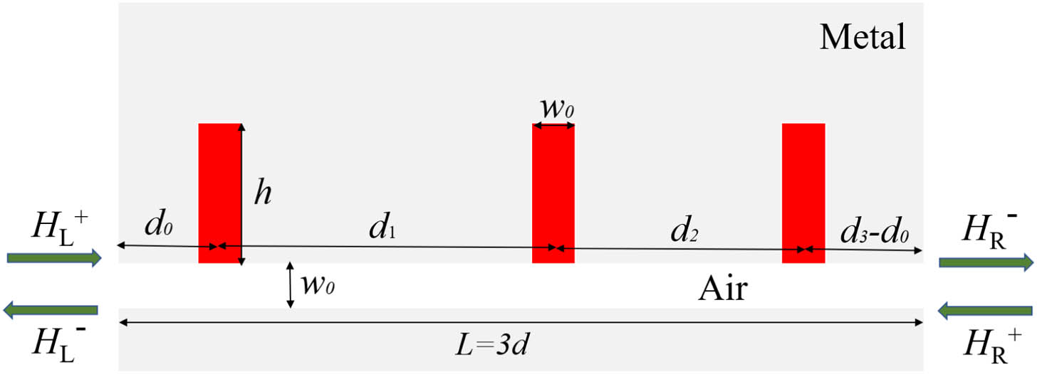
    Fig. 1. Schematic of the compound unit cell of a periodic structure consisting of an MDM waveguide side-coupled to three identical MDM stub resonators.
    (a) Dispersion relation of the periodic structure without modulation calculated using FDFD method (black dots). Results are shown for d1=d2=d3=d=500 nm, h=60 nm, w0=50 nm (Fig. 1), and η=0 [Eq. (1)]. The stubs are filled with InGaAsP with InAs quantum dots, and the metal is silver. Here, we assume that silver is lossless. Also shown is the dispersion relation of a periodic structure with the compound unit cell of Fig. 1, in which the distances between adjacent side-coupled stubs are modulated as in Eq. (1), calculated using FDFD method (red dots). Results are shown for d1=d(1+η cos ϕ), d2=d[1+η cos(2π3+ϕ)], d3=d[1+η cos(4π3+ϕ)], η=0.4, and ϕ=0. All other parameters are the same as in the structure without modulation. (b) Zoomed-in view of the dispersion relation in a narrower frequency range for the periodic structure in which the distances between adjacent side-coupled stubs are modulated. The dispersion relation is calculated using FDFD method (black dots) and CMT (red circles). All other parameters are as in (a).
    Fig. 2. (a) Dispersion relation of the periodic structure without modulation calculated using FDFD method (black dots). Results are shown for d1=d2=d3=d=500  nm, h=60  nm, w0=50  nm (Fig. 1), and η=0 [Eq. (1)]. The stubs are filled with InGaAsP with InAs quantum dots, and the metal is silver. Here, we assume that silver is lossless. Also shown is the dispersion relation of a periodic structure with the compound unit cell of Fig. 1, in which the distances between adjacent side-coupled stubs are modulated as in Eq. (1), calculated using FDFD method (red dots). Results are shown for d1=d(1+ηcosϕ), d2=d[1+ηcos(2π3+ϕ)], d3=d[1+ηcos(4π3+ϕ)], η=0.4, and ϕ=0. All other parameters are the same as in the structure without modulation. (b) Zoomed-in view of the dispersion relation in a narrower frequency range for the periodic structure in which the distances between adjacent side-coupled stubs are modulated. The dispersion relation is calculated using FDFD method (black dots) and CMT (red circles). All other parameters are as in (a).
    (a) Projected dispersion relation of the periodic structure with the compound unit cell of Fig. 1 as a function of ϕ calculated with CMT. The yellow regions correspond to the bands separated by the bandgaps (blue regions). Also shown is the Chern number of each band. The eigenfrequencies of the edge states for right (left) incidence are shown with red (green) dashed line. All other parameters are as in Fig. 2(b). (b) The absolute value of the reflection coefficient |r∞| as a function of ϕ, when the waveguide mode is incident from the right onto the semi-infinite plasmonic structure consisting of compound unit cells as in Fig. 1, calculated using CMT. All parameters are as in (a). (c) The phase θ of the reflection coefficient r∞ as a function of ϕ, when the waveguide mode is incident from the right onto the semi-infinite structure. Also shown is the winding number of each bandgap. All parameters are as in (a).
    Fig. 3. (a) Projected dispersion relation of the periodic structure with the compound unit cell of Fig. 1 as a function of ϕ calculated with CMT. The yellow regions correspond to the bands separated by the bandgaps (blue regions). Also shown is the Chern number of each band. The eigenfrequencies of the edge states for right (left) incidence are shown with red (green) dashed line. All other parameters are as in Fig. 2(b). (b) The absolute value of the reflection coefficient |r| as a function of ϕ, when the waveguide mode is incident from the right onto the semi-infinite plasmonic structure consisting of compound unit cells as in Fig. 1, calculated using CMT. All parameters are as in (a). (c) The phase θ of the reflection coefficient r as a function of ϕ, when the waveguide mode is incident from the right onto the semi-infinite structure. Also shown is the winding number of each bandgap. All parameters are as in (a).
    (a) Reflection spectra when the waveguide mode is incident from the right onto the single-unit-cell structure calculated using the FDFD method (blue solid line). Also shown are the reflection spectra when the waveguide mode is incident from the left (black solid line) and right (red solid line) onto the three-unit-cell structure calculated using the FDFD method. In addition, shown are the calculated reflection spectra using CMT, when the waveguide mode is incident from the right onto the three-unit-cell structure (green circles). Here, the material loss in silver is included. The dielectric constant of the material filling the stubs (InGaAsP with InAs quantum dots) is equal to 11.38+j0.166. All other parameters are as in Fig. 2(b). (b) Profile of the magnetic field amplitude in the middle of the MDM waveguide, normalized with respect to the field amplitude of the incident waveguide mode in the middle of the waveguide, when the mode is incident from the left (black solid line) and right (red solid line) onto the three-unit-cell structure at f=217.5 THz. All other parameters are as in (a). The vertical dashed lines indicate the boundaries between the three-unit-cell structure and the MDM waveguide. (c), (d) Real and imaginary parts of the eigenvalues of the scattering matrix S as a function of frequency. The black and red lines correspond to eigenvalues λs+=t3+r3rr3l and λs−=t3−r3rr3l, respectively. All other parameters are as in (a).
    Fig. 4. (a) Reflection spectra when the waveguide mode is incident from the right onto the single-unit-cell structure calculated using the FDFD method (blue solid line). Also shown are the reflection spectra when the waveguide mode is incident from the left (black solid line) and right (red solid line) onto the three-unit-cell structure calculated using the FDFD method. In addition, shown are the calculated reflection spectra using CMT, when the waveguide mode is incident from the right onto the three-unit-cell structure (green circles). Here, the material loss in silver is included. The dielectric constant of the material filling the stubs (InGaAsP with InAs quantum dots) is equal to 11.38+j0.166. All other parameters are as in Fig. 2(b). (b) Profile of the magnetic field amplitude in the middle of the MDM waveguide, normalized with respect to the field amplitude of the incident waveguide mode in the middle of the waveguide, when the mode is incident from the left (black solid line) and right (red solid line) onto the three-unit-cell structure at f=217.5  THz. All other parameters are as in (a). The vertical dashed lines indicate the boundaries between the three-unit-cell structure and the MDM waveguide. (c), (d) Real and imaginary parts of the eigenvalues of the scattering matrix S as a function of frequency. The black and red lines correspond to eigenvalues λs+=t3+r3rr3l and λs=t3r3rr3l, respectively. All other parameters are as in (a).
    (a), (c) Reflection spectra when the waveguide mode is incident from the right and left, respectively, onto the three-unit-cell structure calculated using the FDFD method. The material loss in silver is included. The dielectric constant of the material filling the stubs (InGaAsP with InAs quantum dots) is equal to 11.38+j0.58. All other parameters are as in Fig. 2(b). (b), (d) Profile of the magnetic field amplitude in the middle of the MDM waveguide, normalized with respect to the field amplitude of the incident waveguide mode in the middle of the waveguide, when the mode is incident from the right and left, respectively, onto the three-unit-cell structure at f=217.5 THz. All other parameters are as in (a). The vertical dashed lines indicate the boundaries between the three-unit-cell structure and the MDM waveguide.
    Fig. 5. (a), (c) Reflection spectra when the waveguide mode is incident from the right and left, respectively, onto the three-unit-cell structure calculated using the FDFD method. The material loss in silver is included. The dielectric constant of the material filling the stubs (InGaAsP with InAs quantum dots) is equal to 11.38+j0.58. All other parameters are as in Fig. 2(b). (b), (d) Profile of the magnetic field amplitude in the middle of the MDM waveguide, normalized with respect to the field amplitude of the incident waveguide mode in the middle of the waveguide, when the mode is incident from the right and left, respectively, onto the three-unit-cell structure at f=217.5  THz. All other parameters are as in (a). The vertical dashed lines indicate the boundaries between the three-unit-cell structure and the MDM waveguide.
    (a) Schematic of the compound unit cell of a structure consisting of a finite number of unit cells. The unit cell consists of an MDM waveguide side-coupled to three MDM stub resonators which have the same resonance frequency ω0 and the same decay rate due to power escape through the waveguide 1τ0, but different decay (growth) rates due to the internal loss (gain) in the stub resonators 1τi,i=1, 2, 3. (b) Reflection spectra when the waveguide mode is incident from the left (black solid line) and right (red solid line) onto a three-unit-cell structure with unit cells as in (a) calculated using the FDFD method. Here, the material loss in silver is included. In each unit cell the first stub is filled with silicon dioxide doped with CdSe quantum dots (ε1=4.0804−j0.0165). The width and length of the first stub are w1=24 nm and h1=90 nm, respectively. The second and third stubs are both filled with InGaAsP with InAs quantum dots (ε2=11.38+j0.346 and ε3=11.38+j0.838). All other parameters are as in Fig. 2(b). (c) Amplitude of the transfer matrix elements |D12|, |D21|, and |D22| as a function of frequency for the three-unit-cell structure of (b).
    Fig. 6. (a) Schematic of the compound unit cell of a structure consisting of a finite number of unit cells. The unit cell consists of an MDM waveguide side-coupled to three MDM stub resonators which have the same resonance frequency ω0 and the same decay rate due to power escape through the waveguide 1τ0, but different decay (growth) rates due to the internal loss (gain) in the stub resonators 1τi,i=1,2,  3. (b) Reflection spectra when the waveguide mode is incident from the left (black solid line) and right (red solid line) onto a three-unit-cell structure with unit cells as in (a) calculated using the FDFD method. Here, the material loss in silver is included. In each unit cell the first stub is filled with silicon dioxide doped with CdSe quantum dots (ε1=4.0804j0.0165). The width and length of the first stub are w1=24  nm and h1=90  nm, respectively. The second and third stubs are both filled with InGaAsP with InAs quantum dots (ε2=11.38+j0.346 and ε3=11.38+j0.838). All other parameters are as in Fig. 2(b). (c) Amplitude of the transfer matrix elements |D12|, |D21|, and |D22| as a function of frequency for the three-unit-cell structure of (b).
    (a), (b) Profile of the magnetic field amplitude in the middle of the MDM waveguide, normalized with respect to the field amplitude of the incident waveguide mode in the middle of the waveguide, when the mode is incident from the left and right, respectively, onto the three-unit-cell structure of Fig. 6(b) at f=217 THz. The vertical dashed lines indicate the boundaries between the three-unit-cell structure and the MDM waveguide. The inset in (a) shows the normalized field profile for 0.1 μm≤X≤0.9 μm, when the waveguide mode is incident from the left.
    Fig. 7. (a), (b) Profile of the magnetic field amplitude in the middle of the MDM waveguide, normalized with respect to the field amplitude of the incident waveguide mode in the middle of the waveguide, when the mode is incident from the left and right, respectively, onto the three-unit-cell structure of Fig. 6(b) at f=217  THz. The vertical dashed lines indicate the boundaries between the three-unit-cell structure and the MDM waveguide. The inset in (a) shows the normalized field profile for 0.1  μmX0.9  μm, when the waveguide mode is incident from the left.
    FOM [Eq. (12)] for the optimized three-unit-cell structure with unit cells as in Fig. 6(a) as a function of frequency. All other parameters are as in Fig. 6(b).
    Fig. 8. FOM [Eq. (12)] for the optimized three-unit-cell structure with unit cells as in Fig. 6(a) as a function of frequency. All other parameters are as in Fig. 6(b).
    Yin Huang, Yuecheng Shen, Georgios Veronis. Topological edge states at singular points in non-Hermitian plasmonic systems[J]. Photonics Research, 2022, 10(3): 747
    Download Citation