• Photonics Research
  • Vol. 10, Issue 3, 747 (2022)
Yin Huang1、5、*, Yuecheng Shen2、6、*, and Georgios Veronis3、4
Author Affiliations
  • 1Department of Optoelectrics Information Science and Engineering, School of Physics and Electronics, Central South University, Changsha 410012, China
  • 2State Key Laboratory of Optoelectronic Materials and Technologies, School of Electronics and Information Technology, Sun Yat-sen University, Guangzhou 510275, China
  • 3School of Electrical Engineering and Computer Science, Louisiana State University, Baton Rouge, Louisiana 70803, USA
  • 4Center for Computation and Technology, Louisiana State University, Baton Rouge, Louisiana 70803, USA
  • 5e-mail: yhuan15@csu.edu.cn
  • 6e-mail: shenyuecheng@mail.sysu.edu.cn
  • show less
    DOI: 10.1364/PRJ.443928 Cite this Article Set citation alerts
    Yin Huang, Yuecheng Shen, Georgios Veronis. Topological edge states at singular points in non-Hermitian plasmonic systems[J]. Photonics Research, 2022, 10(3): 747 Copy Citation Text show less

    Abstract

    We introduce non-Hermitian plasmonic waveguide-cavity systems with topological edge states (TESs) at singular points. The compound unit cells of the structures consist of metal-dielectric-metal (MDM) stub resonators side-coupled to an MDM waveguide. We show that we can realize both a TES and an exceptional point at the same frequency when a proper amount of loss is introduced into a finite three-unit-cell structure. We also show that the finite structure can exhibit both a TES and a spectral singularity when a proper amount of gain is introduced into the structure. In addition, we show that we can simultaneously realize a unidirectional spectral singularity and a TES when proper amounts of loss and gain are introduced into the structure. We finally show that this singularity leads to extremely high sensitivity of the reflected light intensity to variations of the refractive index of the active materials in the structure. TESs at singular points could potentially contribute to the development of singularity-based plasmonic devices with enhanced performance.

    1. INTRODUCTION

    Exceptional points (EPs) are singular points in the spectra of non-Hermitian Hamiltonians in open quantum systems associated with the coalescence of the eigenvalues of the system and their corresponding eigenvectors [1,2]. Unidirectional reflectionless light propagation in non-Hermitian optical systems reveals the presence of EPs [38]. Another type of singular points is spectral singularities (SSs) associated with the lack of completeness of the eigenvectors of non-Hermitian Hamiltonians in the continuous spectra [9,10]. The reflection of non-Hermitian optical systems at SSs tends to infinity and corresponds to lasing at threshold gain [11]. In addition, Ramezani et al. introduced another type of singular points known as unidirectional spectral singularities at which the system exhibits zero reflection from one side and infinite reflection from the opposite side [12]. Singular points can lead to novel optical devices such as optical network analyzers [4], switches [13,14], directional lasers [15], isolators [16], perfect absorbers [17], slow-light waveguides [18], and sensors [1923] with applications in optical computation, communication, and information processing.

    Topological insulators are peculiar electronic materials that possess non-trivial topological states on their edge or surface [24,25]. Topological edge states (TESs) are insensitive to disorder and can lead to field intensity enhancement [24,25]. There have been both theoretical and experimental demonstrations that topological concepts can be transferred to photonics [2630]. Recently, Poshakinskiy et al. demonstrated that TESs can survive in non-Hermitian systems consisting of one-dimensional resonant photonic crystals with modulated couplings, and presented a method to detect these edge states [31]. This opens a pathway to study the connection between TESs and EPs. Most recently, Zhu et al. simultaneously observed TESs and EPs in non-Hermitian acoustic systems with judiciously tailored losses [32]. It would be interesting to investigate whether it is possible to realize both a TES and an EP at the same frequency in non-Hermitian optical systems. In addition, to date the connection between edge states and other types of singular points, such as spectral singularities, has not been explored. It would also be interesting to consider simultaneously realizing edge states and other types of singular points in non-Hermitian optical systems. This could further boost the potential of singular-point-based devices in photonic applications.

    In this paper, we introduce non-Hermitian plasmonic waveguide-cavity systems with TESs at singular points. We first calculate the eigenfrequencies of TESs in a periodic plasmonic structure based on the Aubry–Andre–Harper (AAH) model with compound unit cells consisting of metal-dielectric-metal (MDM) stub resonators side-coupled to an MDM waveguide. The AAH model is the one-dimensional momentum-space projection of the integer quantum Hall effect, and therefore exhibits non-trivial topological properties [30,33,34]. We show that we can realize both a TES and an EP at the same frequency when a proper amount of loss is introduced into a finite plasmonic structure consisting of three compound unit cells. We also show that the finite structure can exhibit both an TES and an SS at the same frequency when a proper amount of gain is introduced into the structure. In addition, we show that we can simultaneously realize a unidirectional spectral singularity and a TES when proper amounts of loss and gain are introduced into the finite plasmonic structure. We finally show that this singularity can lead to extremely high sensitivity of the reflected light intensity to variations of the refractive index of the active materials in the structure.

    2. MODEL

    Analogous to the AAH model, we consider a periodic plasmonic structure with compound unit cells consisting of MDM stub resonators side-coupled to an MDM waveguide (Fig. 1). Among the different plasmonic waveguiding geometries, MDM plasmonic waveguides have attracted a lot of interest [35] because they support modes with deep subwavelength size over a very broad range of frequencies extending from DC to visible [36] and are relatively easy to fabricate [37]. The compound unit cells consist of N side-coupled MDM stub resonators. The distance between the nth and (n+1)th side-coupled stubs in the compound unit cell is modulated and given by dn=d{1+ηcos[2πb(n1)+ϕ]}.Here, b=1/N, d is the distance without modulation, and η is the modulation strength. Figure 1 shows a compound unit cell with three side-coupled stubs, so that b=1/3 (N=3). In addition, ϕ is an arbitrary phase. When ϕ spans the interval between π and π, one-dimensional problems can be mapped to two-dimensional integer quantum Hall effect problems with the Landau gauge characterized by non-zero Chern numbers [30].

    Schematic of the compound unit cell of a periodic structure consisting of an MDM waveguide side-coupled to three identical MDM stub resonators.

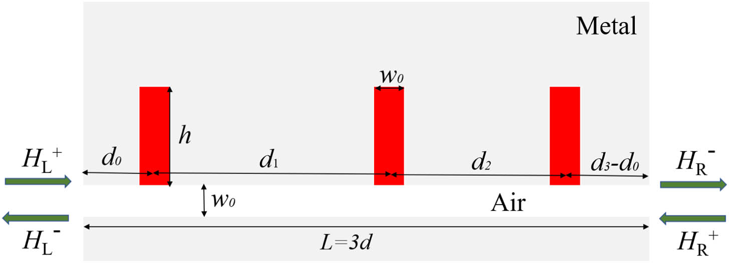
    Figure 1.Schematic of the compound unit cell of a periodic structure consisting of an MDM waveguide side-coupled to three identical MDM stub resonators.

    The periodic system of Fig. 1 can be described by temporal coupled mode theory (CMT) for the mode amplitudes an of the side-coupled stubs, as follows: jωan=(jω01τ01τ)an1τ0nnΛnnan,where ω0 is the resonant frequency, 1τ0 is the decay rate of the stub resonator field due to the power escape through the waveguide, 1τ is the decay (growth) rate due to the internal loss (gain) in the stub resonator, Λnn=eγ|xnxn| with the nth side-coupled stub centered at xn, and γ is the complex propagation constant of the propagating fundamental mode of the MDM waveguide.

    The properties of the compound unit cell of Fig. 1 can be described by the transfer matrix M defined by the following equation: [HRHR+]=M[HL+HL]=[M11M12M21M22][HL+HL],where HL+ and HL are the complex magnetic field amplitudes of the incoming and outgoing modes at the left port, respectively. Similarly, HR+ and HR are the complex magnetic field amplitudes of the incoming and outgoing modes at the right port, respectively (Fig. 1). The transfer matrix M can be calculated by M=M4MsM3MsM2MsM1,where Ms=[tsrs2tsrstsrsts1ts] is the transfer matrix of a system consisting of an MDM waveguide side-coupled to a stub, while rs=1/τ0j(ωω0)+1/τ+1/τ0 and ts=1+rs are the complex reflection and transmission coefficients of the system, respectively [38]. In addition, Mi=[eγLi00eγLi],i=1,2,3,4, where L1=d0, L2=d1, L3=d2, L4=d3d0, and d0 is an arbitrary distance with d0<d3. The transmission coefficient for the compound unit cell is given by t1=HRHL+|HR+=0=HLHR+|HL+=0=M11M12M21M22,while the left and right reflection coefficients for the compound unit cell can be obtained by r1l=HLHL+|HR+=0=M21M22,r1r=HRHR+|HL+=0=M12M22.In addition, the dispersion relation of the periodic plasmonic structure with the compound unit cell of Fig. 1 can be computed using the transfer matrix M of the unit cell and the Bloch boundary conditions HR=ejkLHL+, HR+=ejkLHL by |M[ejkL00ejkL]|=0,where L=3d is the overall length of the compound unit cell (Fig. 1) and k is the Bloch wave vector.

    3. RESULTS

    A. Topological Edge States

    We first consider a periodic plasmonic structure without modulation [η=0 in Eq. (1) so that d1=d2=d3=d]. We choose d=500  nm, h=60  nm, and w0=50  nm (Fig. 1). The metal is silver and the stubs are filled with InGaAsP with InAs quantum dots. In this subsection, we assume that silver is lossless. Please note, however, that the material loss in silver is included in Subsections 3.B–3.D. In the presence of pumping, InGaAsP with InAs quantum dots exhibits optical gain [35,39]. The real part of the dielectric constant of InGaAsP is 11.38 [39]. In Fig. 2(a), we show the dispersion relation of the structure without modulation calculated using the finite-difference frequency-domain (FDFD) method (black dots). The structure supports a middle band corresponding to a mode with slow group velocity. We also consider a structure in which the distances between adjacent side-coupled stubs are modulated as in Eq. (1) with b=1/3, η=0.4, and ϕ=0. The compound unit cell has overall length L=3d (Fig. 1). The middle band with slow group velocity of the structure without modulation [black dots in Fig. 2(a)] splits into three bands due to band mixing for the structure with modulation [red dots in Fig. 2(a)]. Figure 2(b) also shows the dispersion relation of the structure with modulation calculated using CMT [Eq. (7)] (red circles). We observe that there is very good agreement between the CMT results and the exact results obtained using the FDFD method.

    (a) Dispersion relation of the periodic structure without modulation calculated using FDFD method (black dots). Results are shown for d1=d2=d3=d=500 nm, h=60 nm, w0=50 nm (Fig. 1), and η=0 [Eq. (1)]. The stubs are filled with InGaAsP with InAs quantum dots, and the metal is silver. Here, we assume that silver is lossless. Also shown is the dispersion relation of a periodic structure with the compound unit cell of Fig. 1, in which the distances between adjacent side-coupled stubs are modulated as in Eq. (1), calculated using FDFD method (red dots). Results are shown for d1=d(1+η cos ϕ), d2=d[1+η cos(2π3+ϕ)], d3=d[1+η cos(4π3+ϕ)], η=0.4, and ϕ=0. All other parameters are the same as in the structure without modulation. (b) Zoomed-in view of the dispersion relation in a narrower frequency range for the periodic structure in which the distances between adjacent side-coupled stubs are modulated. The dispersion relation is calculated using FDFD method (black dots) and CMT (red circles). All other parameters are as in (a).

    Figure 2.(a) Dispersion relation of the periodic structure without modulation calculated using FDFD method (black dots). Results are shown for d1=d2=d3=d=500  nm, h=60  nm, w0=50  nm (Fig. 1), and η=0 [Eq. (1)]. The stubs are filled with InGaAsP with InAs quantum dots, and the metal is silver. Here, we assume that silver is lossless. Also shown is the dispersion relation of a periodic structure with the compound unit cell of Fig. 1, in which the distances between adjacent side-coupled stubs are modulated as in Eq. (1), calculated using FDFD method (red dots). Results are shown for d1=d(1+ηcosϕ), d2=d[1+ηcos(2π3+ϕ)], d3=d[1+ηcos(4π3+ϕ)], η=0.4, and ϕ=0. All other parameters are the same as in the structure without modulation. (b) Zoomed-in view of the dispersion relation in a narrower frequency range for the periodic structure in which the distances between adjacent side-coupled stubs are modulated. The dispersion relation is calculated using FDFD method (black dots) and CMT (red circles). All other parameters are as in (a).

    Figure 3(a) shows the projected band structure of the periodic structure with the compound unit cell of Fig. 1 for η=0.4 and b=1/3 as a function of the phase ϕ [Eq. (1)], calculated with CMT. For a fixed ϕ, we have three bands (yellow regions) in the frequency range of interest. As an example, for ϕ=0 the system supports three bands with frequencies ranging from 192 to 195 THz, 214 to 215 THz, and 221 to 235 THz [Figs. 2(b) and 3(a)]. As the phase ϕ varies from π to π, the Bloch eigenstates of the system are a function of k and ϕ. Thus, each band is characterized by a Chern number which is defined as 12πjππdϕπ/Lπ/Ldk(kAϕϕAk), where Ak=sas*kas, Aϕ=sas*ϕas, and as,s=1,2,3 are the mode amplitudes satisfying the Bloch condition as+3l(k,ϕ)=ejlkLas(k,ϕ) for l=0,±1,±2,. This Chern number can also be deduced from the winding number of the bandgap using the phase of the reflection coefficient for the semi-infinite structure [32,40]. Imposing the Bloch boundary condition, the reflection coefficient for the semi-infinite structure r, when the waveguide mode is incident from the right, can be obtained using the transfer matrix r=ejkLM22M21.Note that, in the lossless case, the left and right reflection coefficients are equal.

    (a) Projected dispersion relation of the periodic structure with the compound unit cell of Fig. 1 as a function of ϕ calculated with CMT. The yellow regions correspond to the bands separated by the bandgaps (blue regions). Also shown is the Chern number of each band. The eigenfrequencies of the edge states for right (left) incidence are shown with red (green) dashed line. All other parameters are as in Fig. 2(b). (b) The absolute value of the reflection coefficient |r∞| as a function of ϕ, when the waveguide mode is incident from the right onto the semi-infinite plasmonic structure consisting of compound unit cells as in Fig. 1, calculated using CMT. All parameters are as in (a). (c) The phase θ of the reflection coefficient r∞ as a function of ϕ, when the waveguide mode is incident from the right onto the semi-infinite structure. Also shown is the winding number of each bandgap. All parameters are as in (a).

    Figure 3.(a) Projected dispersion relation of the periodic structure with the compound unit cell of Fig. 1 as a function of ϕ calculated with CMT. The yellow regions correspond to the bands separated by the bandgaps (blue regions). Also shown is the Chern number of each band. The eigenfrequencies of the edge states for right (left) incidence are shown with red (green) dashed line. All other parameters are as in Fig. 2(b). (b) The absolute value of the reflection coefficient |r| as a function of ϕ, when the waveguide mode is incident from the right onto the semi-infinite plasmonic structure consisting of compound unit cells as in Fig. 1, calculated using CMT. All parameters are as in (a). (c) The phase θ of the reflection coefficient r as a function of ϕ, when the waveguide mode is incident from the right onto the semi-infinite structure. Also shown is the winding number of each bandgap. All parameters are as in (a).

    Figure 3(b) shows the absolute value of the reflection coefficient |r| calculated using Eq. (8), when the waveguide mode is incident from the right onto the semi-infinite plasmonic structure consisting of compound unit cells as in Fig. 1. We observe that |r| shown in Fig. 3(b) is consistent with the dispersion relation shown in Fig. 3(a). The absolute value of the reflection coefficient |r| for frequencies lying inside the bandgaps is 1 [Fig. 3(b)]. Hence, the reflection coefficient r for frequencies lying inside the bandgaps is 1×ejθ, where θ is the phase of the reflection coefficient. The winding number, which is the topological invariant of the bandgap, can thus be calculated using [41] w=12πj02πln[r(ϕ)]ϕdϕ=12π02πθ(ϕ).

    Figure 3(c) shows the phase θ of the reflection coefficient r when the waveguide mode is incident from the right onto the semi-infinite structure. The extra phase that the reflection coefficient accumulates when ϕ varies from π to π is 0, 2π, 2π, and 0 for the first, second, third, and fourth bandgaps, respectively, in the frequency range of interest. The winding numbers of these four bandgaps are therefore 0, 1, −1, and 0 [Eq. (9)]. Thus, since the Chern number of a band is equal to the winding number of the above-lying bandgap minus the winding number of below-lying bandgap [40], the Chern numbers of the three bands in the frequency range of interest are 1, 2, and 1 [Fig. 3(a)]. Non-zero Chern numbers indicate the existence of TESs in the bandgaps based on the bulk-boundary correspondence [41].

    The TESs can be obtained by direct calculation of Eq. (2). However, this calculation is challenging since Λnn depends on the frequency ω. Alternatively, the TESs can be extracted from the zeros of the reflection coefficient r when an appropriate amount of loss (1τ>0) is introduced into the semi-infinite structure; that is, r(ω,1τ)=0 [31,32]. The underlying physical mechanism behind this can be explained as follows: when light with the eigenfrequency of the edge state is incident on the structure, the edge state is excited and the light is deeply trapped in the edge region. If an appropriate amount of loss is introduced into the system, the trapped light is completely absorbed, and thus r(ω,1τ)=0. The zeros of r(ω,1τ) are identical to the zeros of r1(ω,1τ) for a unit cell [32]. More specifically, if one considers the transfer matrix of a unit cell with r1l=0 (r1r=0), then by calculating the transfer matrix for m unit cells, one can show that rml=0 (rmr=0) [32]. Thus, the eigenfrequencies of the left and right edge states can be retrieved from r1l(ω,1τ)=0 and r1r(ω,1τ)=0, respectively. Figure 3(a) shows that the structure possesses two chiral edge states in each bandgap. The green dashed line corresponds to the left edge state [r1l(ω,1τ)=0], while the red dashed line corresponds to the right edge state [r1r(ω,1τ)=0].

    In a two-dimensional quantum Hall system, edge states exhibit chirality, so that edge states at opposite edges propagate in opposite directions [41]. The AAH model is the one-dimensional momentum-space projection of the integer quantum Hall effect. The modulation distance in Eq. (1) provides an effective gauge magnetic field, and the phase ϕ accounts for the momentum along the geometrical dimension that was lost when moving from a two-dimensional to a one-dimensional system. A consequence of chirality in the one-dimensional AAH model is that in a given structure with a specific phase ϕ left and right edge states cannot be excited at the same frequency.

    B. Topological Edge States at Exceptional Points

    In this subsection, to realize both a TES and an EP at the same frequency, we consider a finite structure consisting of three compound unit cells as in Fig. 1 with ϕ=0 [Eq. (1)]. The number of unit cells is chosen so that the structure is sufficiently long to form a bandgap, and the TESs can appear within this bandgap [32]. On the other hand, the location of the singular points is determined by the unit cell properties, so that the number of unit cells in the structure does not affect their location. As shown in Fig. 3(a), a right TES exists in the second bandgap around ϕ=0 (red dashed line), when a proper amount of loss is introduced into the system. More specifically, when the waveguide mode is incident onto a single-unit-cell structure from the right, we find using CMT that r1r=0 for decay rate due to internal loss in the stub resonators with 1/τ equal to 8.77×10¹²  s1. We also find that, when we take into account the material loss of silver, the material filling the stubs (InGaAsP with InAs quantum dots) must exhibit gain with the imaginary part of its dielectric constant equal to 0.166, in order for 1/τ to be equal to 8.77×10¹²  s1. Figure 4(a) confirms that the reflection, when the waveguide mode is incident from the right onto the single-unit-cell structure, calculated using the FDFD method (blue solid line) becomes zero (r1r=0) for the dielectric constant of the material filling the stubs equal to 11.38+j0.166 at the frequency of f=217.5  THz. We also find that the calculated reflection using the FDFD method, when the waveguide mode is incident from the right onto the three-unit-cell structure (red solid line), becomes zero (r3r=0) at the same frequency (f=217.5  THz) as the single-unit-cell structure [Fig. 4(a)]. Thus, we conclude that there exists a TES localized at the right boundary of the three-unit-cell structure for f=217.5  THz. Figure 4(a) also shows the calculated reflection using CMT, when the waveguide mode is incident from the right onto the three-unit-cell structure (green circles). Once again, we observe that there is very good agreement between the CMT results and the exact results obtained using the FDFD method.

    (a) Reflection spectra when the waveguide mode is incident from the right onto the single-unit-cell structure calculated using the FDFD method (blue solid line). Also shown are the reflection spectra when the waveguide mode is incident from the left (black solid line) and right (red solid line) onto the three-unit-cell structure calculated using the FDFD method. In addition, shown are the calculated reflection spectra using CMT, when the waveguide mode is incident from the right onto the three-unit-cell structure (green circles). Here, the material loss in silver is included. The dielectric constant of the material filling the stubs (InGaAsP with InAs quantum dots) is equal to 11.38+j0.166. All other parameters are as in Fig. 2(b). (b) Profile of the magnetic field amplitude in the middle of the MDM waveguide, normalized with respect to the field amplitude of the incident waveguide mode in the middle of the waveguide, when the mode is incident from the left (black solid line) and right (red solid line) onto the three-unit-cell structure at f=217.5 THz. All other parameters are as in (a). The vertical dashed lines indicate the boundaries between the three-unit-cell structure and the MDM waveguide. (c), (d) Real and imaginary parts of the eigenvalues of the scattering matrix S as a function of frequency. The black and red lines correspond to eigenvalues λs+=t3+r3rr3l and λs−=t3−r3rr3l, respectively. All other parameters are as in (a).

    Figure 4.(a) Reflection spectra when the waveguide mode is incident from the right onto the single-unit-cell structure calculated using the FDFD method (blue solid line). Also shown are the reflection spectra when the waveguide mode is incident from the left (black solid line) and right (red solid line) onto the three-unit-cell structure calculated using the FDFD method. In addition, shown are the calculated reflection spectra using CMT, when the waveguide mode is incident from the right onto the three-unit-cell structure (green circles). Here, the material loss in silver is included. The dielectric constant of the material filling the stubs (InGaAsP with InAs quantum dots) is equal to 11.38+j0.166. All other parameters are as in Fig. 2(b). (b) Profile of the magnetic field amplitude in the middle of the MDM waveguide, normalized with respect to the field amplitude of the incident waveguide mode in the middle of the waveguide, when the mode is incident from the left (black solid line) and right (red solid line) onto the three-unit-cell structure at f=217.5  THz. All other parameters are as in (a). The vertical dashed lines indicate the boundaries between the three-unit-cell structure and the MDM waveguide. (c), (d) Real and imaginary parts of the eigenvalues of the scattering matrix S as a function of frequency. The black and red lines correspond to eigenvalues λs+=t3+r3rr3l and λs=t3r3rr3l, respectively. All other parameters are as in (a).

    In addition, we find that for the three-unit-cell structure the reflection for the waveguide mode incident from the right (red solid line) is zero at f=217.5  THz, while the reflection for the waveguide mode incident from the left (black solid line) is non-zero [Fig. 4(a)]. Thus, the structure exhibits unidirectional reflectionless propagation at f=217.5  THz. The properties of the three-unit-cell structure can also be described by the scattering matrix S=[t3r3rr3lt3]. The matrix S is non-Hermitian in the presence of loss, and its complex eigenvalues are λs±=t3±r3rr3l. The corresponding eigenstates, which are ψ±=(1,±r3rr3l) for r3l0, are not orthogonal [8]. In the case of unidirectional reflectionless propagation in the right direction (r3r=0,r3l0), both the scattering matrix S eigenvalues and their corresponding eigenstates coalesce, and thus an EP is formed. In other words, the three-unit-cell structure exhibits both a TES and an EP at the same frequency. In addition, we can observe both the localized TES and the unidirectional reflectionless propagation in the normalized magnetic field distributions at that frequency. When the waveguide mode is incident from the left, there is strong reflection, so that the incident and reflected modal fields form a strong interference pattern [Fig. 4(b)]. On the other hand, when the waveguide mode is incident from the right, there is hardly any reflection. In addition, the field is enhanced at the right edge, demonstrating the existence of the edge state [Fig. 4(b)]. In Figs. 4(c) and 4(d) we show the real and imaginary parts, respectively, of the eigenvalues of the scattering matrix S as a function of frequency. We observe that the real and imaginary parts of the two eigenvalues indeed collapse at the exceptional point (f=217.5  THz). In Figs. 4(c) and 4(d), we also observe a level repulsion in the real parts of the eigenvalues, as well as a level crossing in their imaginary parts [6].

    C. Topological Edge States at Spectral Singularities

    Another type of singular points is spectral singularities which, unlike EPs, can only occur in the presence of gain [9]. An optical system which supports an SS has purely outgoing radiation, that is, HL+=HR+=0, HL0, and HR0 (Fig. 1), so that it acts as a laser. If these conditions are satisfied, we have M22=0 [Eq. (3)]. The reflection of non-Hermitian optical systems at SSs tends to infinity [11]. Based on Eqs. (3), (4), and (8), the reflection coefficient for the semi-infinite structure r depends on the reflection coefficient for the single stub structure rs which is a function of ωj1τ. The winding number of a bandgap can thus be written as a function of ωj1τ: w(ωj1τ)=12πj02πln[r(ωj1τ,ϕ)]ϕdϕ.In the lossless case (1τ=0), the winding number of the third bandgap is 1 [Fig. 3(c)]. On the other hand, for 1τ, rs=1/τ0j(ωω0)+1/τ+1/τ00, which indicates that the waveguide-cavity structure reduces to a straight waveguide. The reflection coefficient r therefore becomes zero and is independent of ϕ. Thus, based on Eq. (10), lim1τw=0. Since the winding number as a topological invariant is an integer, its value must abruptly change from −1 to 0 at certain finite 1τ(0,). Such a discontinuity can only be caused by a singularity of the integrand in Eq. (10), which corresponds to a zero of the reflection coefficient r, that is, r(ωj1τ)=0 [40]. In the lossless case (1τ=0), |r|2=1 for frequencies lying inside the bandgap. In the presence of loss, |r|2=1 turns into r(ωj1τ)r*(ω+j1τ)=1. Since r(ωj1τ)=0, we must have r(ω+j1τ). In other words, if the reflection in the semi-infinite structure tends to infinity when a proper amount of gain is introduced, the structure exhibits a TES. In addition, such a pole of the reflection coefficient r corresponds to the presence of an SS [11]. Thus, this analysis suggests that, if a proper amount of gain is introduced into the structure, it can exhibit both a TES and an SS at the same frequency.

    To implement this in plasmonic waveguide-cavity systems as in Fig. 1, we consider as before a finite structure consisting of three compound unit cells with ϕ=0 for d=500  nm, h=60  nm, w0=50  nm, and η=0.4 [Eq. (1)]. Using CMT, we find that the reflection coefficient for the waveguide mode incident onto the finite structure from the right |r3r| tends to infinity, when the decay rate of the stub resonator mode amplitude 1τ approximately equals 1.37×10¹³  s1. To satisfy this condition we find that, when we take into account the material loss of silver, the material filling the stubs (InGaAsP with InAs quantum dots) must exhibit gain with the imaginary part of its dielectric constant equal to 0.58. Figure 5(a) shows that the calculated reflection using the FDFD method when the waveguide mode is incident from the right onto the three-unit-cell structure becomes extremely large for the dielectric constant of the material filling the stubs equal to 11.38+j0.58 at f=217.5  THz. This result indicates that a TES exists at the right boundary of the structure for f=217.5  THz. In addition, the narrow-width resonance corresponding to a lasing process suggests that the structure exhibits an SS. The TES and right lasing can also be observed in the normalized magnetic field distributions at the SS [Fig. 5(b)]. When the waveguide mode is incident from the right, the reflected fields are greatly amplified. In addition, the greatly enhanced field at the right edge of the structure confirms the existence of the edge state. In contrast to the incidence from the right side, the reflection from the left side does not diverge at f=217.5  THz [Fig. 5(c)]. In addition, no TES exists at the left boundary of the structure [Fig. 5(d)].

    (a), (c) Reflection spectra when the waveguide mode is incident from the right and left, respectively, onto the three-unit-cell structure calculated using the FDFD method. The material loss in silver is included. The dielectric constant of the material filling the stubs (InGaAsP with InAs quantum dots) is equal to 11.38+j0.58. All other parameters are as in Fig. 2(b). (b), (d) Profile of the magnetic field amplitude in the middle of the MDM waveguide, normalized with respect to the field amplitude of the incident waveguide mode in the middle of the waveguide, when the mode is incident from the right and left, respectively, onto the three-unit-cell structure at f=217.5 THz. All other parameters are as in (a). The vertical dashed lines indicate the boundaries between the three-unit-cell structure and the MDM waveguide.

    Figure 5.(a), (c) Reflection spectra when the waveguide mode is incident from the right and left, respectively, onto the three-unit-cell structure calculated using the FDFD method. The material loss in silver is included. The dielectric constant of the material filling the stubs (InGaAsP with InAs quantum dots) is equal to 11.38+j0.58. All other parameters are as in Fig. 2(b). (b), (d) Profile of the magnetic field amplitude in the middle of the MDM waveguide, normalized with respect to the field amplitude of the incident waveguide mode in the middle of the waveguide, when the mode is incident from the right and left, respectively, onto the three-unit-cell structure at f=217.5  THz. All other parameters are as in (a). The vertical dashed lines indicate the boundaries between the three-unit-cell structure and the MDM waveguide.

    D. Topological Edge States at Unidirectional Spectral Singularities

    A unidirectional spectral singularity is a singular point at which zero reflection from one side and infinite reflection from the opposite side are simultaneously realized [12]. As we saw in Subsection 3.C, the edge state at the SS shows up as a narrow-width resonance in the reflection spectra when a proper amount of gain is introduced into the stub resonators. Based on Eqs. (6) and (8), it is possible that the reflection coefficient in the right direction for the semi-infinite structure r approaches infinity, and the reflection coefficient in the left direction for the structure consisting of a single unit cell is zero. This suggests that a properly designed structure could exhibit both a TES and a unidirectional spectral singularity at the same frequency.

    To implement this in plasmonic waveguide-cavity systems, we consider a compound unit cell with three stubs which have the same resonance frequency ω0 and the same decay rate due to power escape through the waveguide 1τ0, but different decay (growth) rates due to the internal loss (gain) in the stub resonators 1τi,i=1,  2,  3 [Fig. 6(a)]. We consider as before a finite structure consisting of three compound unit cells with ϕ=0, d=500  nm, and η=0.4 [Eq. (1)]. Recall that the zeros of the reflection coefficient for the single-unit-cell structure r1 are identical to the zeros of the reflection coefficient for the three-unit-cell structure r3. We first use CMT to optimize the decay (growth) rates due to internal loss (gain) of all three stubs 1τi,i=1,2,  3, to simultaneously make the amplitude of the transfer matrix element M21 as close to zero as possible, and the amplitude of the reflection coefficient in the right direction for the three-unit-cell structure r3r as large as possible. Using this approach, we find that M21 vanishes and r3r diverges for 1τ1=2.21×10¹³  s1, 1τ2=1.81×10¹¹  s1, and 1τ3=2.86×10¹³  s1. Thus, the first two stubs in the compound unit cell exhibit loss, while the third one exhibits gain. Figure 6(b) shows the reflection spectra for the optimized three-unit-cell structure calculated using the FDFD method for incident waveguide modes from both the left and right directions. At f=217  THz the reflection from the left (black) is close to zero, while the reflection from the right (red) tends to infinity. In other words, the optimized structure simultaneously supports a unidirectional spectral singularity, as well as a TES on the right edge at f=217  THz.

    (a) Schematic of the compound unit cell of a structure consisting of a finite number of unit cells. The unit cell consists of an MDM waveguide side-coupled to three MDM stub resonators which have the same resonance frequency ω0 and the same decay rate due to power escape through the waveguide 1τ0, but different decay (growth) rates due to the internal loss (gain) in the stub resonators 1τi,i=1, 2, 3. (b) Reflection spectra when the waveguide mode is incident from the left (black solid line) and right (red solid line) onto a three-unit-cell structure with unit cells as in (a) calculated using the FDFD method. Here, the material loss in silver is included. In each unit cell the first stub is filled with silicon dioxide doped with CdSe quantum dots (ε1=4.0804−j0.0165). The width and length of the first stub are w1=24 nm and h1=90 nm, respectively. The second and third stubs are both filled with InGaAsP with InAs quantum dots (ε2=11.38+j0.346 and ε3=11.38+j0.838). All other parameters are as in Fig. 2(b). (c) Amplitude of the transfer matrix elements |D12|, |D21|, and |D22| as a function of frequency for the three-unit-cell structure of (b).

    Figure 6.(a) Schematic of the compound unit cell of a structure consisting of a finite number of unit cells. The unit cell consists of an MDM waveguide side-coupled to three MDM stub resonators which have the same resonance frequency ω0 and the same decay rate due to power escape through the waveguide 1τ0, but different decay (growth) rates due to the internal loss (gain) in the stub resonators 1τi,i=1,2,  3. (b) Reflection spectra when the waveguide mode is incident from the left (black solid line) and right (red solid line) onto a three-unit-cell structure with unit cells as in (a) calculated using the FDFD method. Here, the material loss in silver is included. In each unit cell the first stub is filled with silicon dioxide doped with CdSe quantum dots (ε1=4.0804j0.0165). The width and length of the first stub are w1=24  nm and h1=90  nm, respectively. The second and third stubs are both filled with InGaAsP with InAs quantum dots (ε2=11.38+j0.346 and ε3=11.38+j0.838). All other parameters are as in Fig. 2(b). (c) Amplitude of the transfer matrix elements |D12|, |D21|, and |D22| as a function of frequency for the three-unit-cell structure of (b).

    In each compound unit cell, the first stub is filled with silicon dioxide doped with CdSe quantum dots (ε1=4.0804j0.0165). This active absorbing material is tunable, since the imaginary part of its refractive index can be modified with an external control beam [42,43]. The width and length of the first stub are w1=24  nm and h1=90  nm, respectively. The second and third stubs are both filled with InGaAsP with InAs quantum dots but have dielectric constants with different imaginary parts (ε2=11.38+j0.346 and ε3=11.38+j0.838). The widths and lengths of these two stubs are w2=w3=50  nm and h2=h3=60  nm as before. As mentioned above, we choose the stub dimensions so that their resonance frequencies as well as their decay rates due to power escape through the waveguide are equal. In addition, taking into account the material loss of silver, we choose the imaginary parts of the dielectric constants of the materials filling the three stubs so as to satisfy the conditions 1τ1=2.21×10¹³  s1, 1τ2=1.81×10¹¹  s1, and 1τ3=2.86×10¹³  s1, which, as mentioned above, were obtained using CMT.

    If the overall transfer matrix of the optimized three-unit-cell structure is D=[D11D12D21D22], then the reflection coefficients for the left and right directions are given by D21D22 and D12D22, respectively. A unidirectional reflectionless propagating mode for incidence from one side, as well as a unidirectional lasing mode for incidence from the other side, is the key signature of a unidirectional spectral singularity. This exotic response has also been observed in PT-symmetric coupled cavity systems [12]. In these systems, such a phenomenon is obtained for D12, D210, and D220 at the operating frequency [12]. Figure 6(c) shows the amplitudes of the transfer matrix elements |D21|, |D12|, and |D22| as a function of frequency for our optimized three-unit-cell structure. We observe that, in contrast to the PT-symmetric coupled cavity systems [12], the unidirectional spectral singularity in our case is obtained through D120,D210,D220.D120 and D220 [Fig. 6(c)] lead to diverging reflection from the right side at f=217  THz [Fig. 6(b)]. D21 approaching zero faster than D22 [Fig. 6(c)] results in vanishing reflection from the left side at f=217  THz [Fig. 6(b)].

    In addition, we can observe both the TES and the unidirectional spectral singularity in the normalized magnetic field distributions for the optimized structure of Fig. 6(a) at f=217  THz [Figs. 7(a) and 7(b)]. When the waveguide mode is incident from the left, there is hardly any reflection, as seen in Fig. 7(a) and its inset. When the waveguide mode is incident from the right, the reflected wave is enhanced by 3 orders of magnitude [Fig. 7(b)]. In addition, the significantly enhanced field at the right edge of the structure verifies the existence of the edge state. In the previously reported PT-symmetric coupled cavity system [12], the main mechanism to create a unidirectional spectral singularity was based on Fano resonance trapping in the system. Light reflected from the gain side is strongly confined in the gain cavity and amplified, while light reflected from the lossy side is trapped in the lossy cavity and absorbed [12]. In our case, the right lasing is caused by the topologically protected edge mode localization on the gain side (right side). However, due to the chirality of TESs in our system, there is no edge state on the lossy side (left side). The left reflectionlessness of our structure is originating from destructive interference rather than from light trapping. Thus, we observe that the field profiles in Figs. 7(a) and 7(b) are very similar except that the field enhancement is much larger for waveguide modes incident from the right. It is worth noting that in this case the zero reflection in the left direction is not the signature of a TES on the left side, since the optimized structure includes a gain stub with 1τ<0. The zero reflection from the left side is associated with destructive interference rather than with light trapping at the left edge of the structure.

    (a), (b) Profile of the magnetic field amplitude in the middle of the MDM waveguide, normalized with respect to the field amplitude of the incident waveguide mode in the middle of the waveguide, when the mode is incident from the left and right, respectively, onto the three-unit-cell structure of Fig. 6(b) at f=217 THz. The vertical dashed lines indicate the boundaries between the three-unit-cell structure and the MDM waveguide. The inset in (a) shows the normalized field profile for 0.1 μm≤X≤0.9 μm, when the waveguide mode is incident from the left.

    Figure 7.(a), (b) Profile of the magnetic field amplitude in the middle of the MDM waveguide, normalized with respect to the field amplitude of the incident waveguide mode in the middle of the waveguide, when the mode is incident from the left and right, respectively, onto the three-unit-cell structure of Fig. 6(b) at f=217  THz. The vertical dashed lines indicate the boundaries between the three-unit-cell structure and the MDM waveguide. The inset in (a) shows the normalized field profile for 0.1  μmX0.9  μm, when the waveguide mode is incident from the left.

    Very recently, high-sensitivity sensors based on EPs with topological edge states in non-Hermitian chains have been proposed and experimentally demonstrated [44,45]. The extremely sharp line shape of the reflection from the left side [Fig. 6(b)] provides an opportunity to design an extremely sensitive active structure at the unidirectional spectral singularity. To characterize the sensitivity of the optimized three-unit-cell structure with unit cells as in Fig. 6(a), we define the figure of merit (FOM) as the absolute value of the derivative of the reflection from the left R3l with respect to the imaginary part κ of the refractive index of the active absorbing material filling the first stub of each unit cell [Fig. 6(a)] divided by R3l: FOM=|dR3lR3ldκ|,where R3l=|r3l|2. High sensitivity with respect to the imaginary part of the refractive index could have applications in optical switches and modulators [46]. The FOM can be calculated using the following finite-difference approximation: dR3ldκR3l(κ+Δκ)R3l(κΔκ)2Δκ. In our calculations, we use Δκ=0.25×10⁴κ [47]. Figure 8 shows the calculated FOM as a function of frequency. The maximum value of the FOM is 160,000 at the unidirectional spectral singularity (f=217  THz), which is more than 2 orders of magnitude larger than the FOM in plasmonic sensors based on the Fano resonance [48]. We found that the unidirectional spectral singularity also leads to extremely high sensitivity to variations of the real part of the refractive index. We also found that, as the number of unit cells increases, the FOM increases.

    FOM [Eq. (12)] for the optimized three-unit-cell structure with unit cells as in Fig. 6(a) as a function of frequency. All other parameters are as in Fig. 6(b).

    Figure 8.FOM [Eq. (12)] for the optimized three-unit-cell structure with unit cells as in Fig. 6(a) as a function of frequency. All other parameters are as in Fig. 6(b).

    We note that our choice for the imaginary part of the refractive index of the active absorbing material (κ=4.08×10³) is within the range of experimentally achievable values [42,43,46]. In addition, the imaginary parts of the dielectric constant of the gain material filling the second and third stubs of each unit cell in the optimized structure [Fig. 6(a)] are 0.346 and 0.838, respectively, which correspond to gain coefficients of g4666  cm1 and g11,250  cm1, respectively [49]. These can be realized with ultra-high-density quantum dot structures [50,51].

    4. CONCLUSIONS

    In this paper, we focused on non-Hermitian nano-optic systems, and first investigated the connection between TESs and EPs in such systems. We also explored the connection between TESs and other types of singular points, such as SSs and unidirectional spectral singularities, in nano-optic systems. We finally explored the potential of nano-optic structures which exhibit both TESs and singular points in sensing.

    More specifically, we designed non-Hermitian periodic plasmonic waveguide-cavity structures based on the AAH model to realize both a TES and a singular point at the same frequency. We used the transfer matrix method and CMT to account for the behavior of the proposed structures. We first showed that we can realize both an TES and an EP at the same frequency when a proper amount of loss is introduced into the plasmonic structure. We also showed that the structure can exhibit both a TES and an SS at the same frequency when a proper amount of gain is introduced into the structure. Thus, the system acts as a topological laser. Unlike previous works that used two-dimensional photonic structures to realize topological lasers [5254], we used a one-dimensional structure based on the AAH model. In addition, we showed that we can realize both unidirectional spectral singularities and TESs when a proper amount of loss and gain are introduced into the plasmonic structure. The optimized structure supports unidirectional reflectionless propagation for incidence from one side, as well as a unidirectional lasing for incidence from the other side. The underlying physical mechanism of the unidirectional lasing is the topologically protected edge mode localization on the gain side, while the unidirectional reflectionlessness is originating from destructive interference. Finally, we found that for such a structure the sensitivity of the reflection to variations of the refractive index of the active material, when the waveguide mode is incident from the side which supports unidirectional reflectionlessness, is significantly enhanced at the unidirectional spectral singularity. Thus, the optimized structure operating at the unidirectional spectral singularity can lead to extremely sensitive active photonic devices such as modulators and switches.

    As final remarks, we expect the singular points associated with TESs to be robust in the presence of disorder, as long as the disorder is not strong enough to close the bandgaps [Fig. 3(a)]. To test this hypothesis, we randomly varied the distances between adjacent stubs in our proposed three-unit-cell structure with variations which are uniformly distributed over the interval (40  nm, 40 nm). We first considered the robustness of structures exhibiting both EPs and TESs at the same frequency. We confirmed that in such structures both the EPs and the TESs are robust in the presence of disorder. We also considered the robustness of structures exhibiting both SSs and TESs at the same frequency. We again confirmed that in such structures both the SSs and the TESs are robust in the presence of disorder. We also note that singular points such as EPs, SSs, and unidirectional spectral singularities can also be achieved in single-unit-cell structures [6,17]. Unlike the singular points in single-unit-cell structures, the singular points associated with TESs in our proposed structures are robust in the presence of disorder.

    We note that the AAH model can also be realized in two-dimensional photonic crystal structures [55]. We also note that the one-dimensional AAH model exhibits phenomena associated with the two-dimensional integer quantum Hall effect. The same concept could be generalized to two-dimensional quasicrystals and be used to realize an analog of the four-dimensional integer quantum Hall effect [56,57]. The two-dimensional quasicrystal system could support topological corner states to realize topologically protected singular points.

    Our results demonstrate the connection between topologically protected edge states and different types of singular points and could potentially contribute to the development of a new generation of singularity-based plasmonic devices with enhanced performance. The concept of combining gain and loss to realize both TESs and singular points at the same frequency could also be applied in other photonic and acoustic systems. In addition, we note that TESs at singular points could be realized in three-dimensional plasmonic waveguide-cavity systems based on plasmonic coaxial waveguides [58,59].

    References

    [1] N. Moiseyev. Non-Hermitian Quantum Mechanics(2011).

    [2] W. Heiss. Exceptional points of non-Hermitian operators. J. Phys. A, 37, 2455-2464(2004).

    [3] Z. Lin, H. Ramezani, T. Eichelkraut, T. Kottos, H. Cao, D. N. Christodoulides. Unidirectional invisibility induced by PT-symmetric periodic structures. Phys. Rev. Lett., 106, 213901(2011).

    [4] L. Feng, Y. L. Xu, W. S. Fegadolli, M. H. Lu, J. E. B. Oliveira, V. R. Almeida, Y. F. Chen, A. Scherer. Experimental demonstration of a unidirectional reflectionless parity-time metamaterial at optical frequencies. Nat. Mater., 12, 108-113(2013).

    [5] L. Ge, Y. D. Chong, A. D. Stone. Conservation relations and anisotropic transmission resonances in one-dimensional PT-symmetric photonic heterostructures. Phys. Rev. Lett., 85, 023802(2012).

    [6] Y. Huang, G. Veronis, C. Min. Unidirectional reflectionless propagation in plasmonic waveguide-cavity systems at exceptional points. Opt. Express, 23, 29882-29895(2015).

    [7] X. Yin, X. Zhang. Unidirectional light propagation at exceptional points. Nat. Mater., 12, 175-177(2013).

    [8] Y. Huang, Y. Shen, C. Min, S. Fan, G. Veronis. Unidirectional reflectionless light propagation at exceptional points. Nanophotonics, 6, 977-996(2017).

    [9] A. Mostafazadeh. Spectral singularities of complex scattering potentials and infinite reflection and transmission coefficients at real energies. Phys. Rev. Lett., 102, 220402(2009).

    [10] V. V. Konotop, D. A. Zezyulin. Spectral singularities of odd-PT-symmetric potentials. Phys. Rev. A, 99, 013823(2019).

    [11] A. Mostafazadeh. Optical spectral singularities as threshold resonances. Phys. Rev. A, 83, 045801(2011).

    [12] H. Ramezani, H. Li, Y. Wang, X. Zhang. Unidirectional spectral singularities. Phys. Rev. Lett., 113, 263905(2014).

    [13] J. Doppler, A. Mailybaev, J. Bohm, U. Kuhl, A. Girschik, F. Libisch, T. Milburn, P. Rabl, N. Moiseyev, S. Rotter. Dynamically encircling an exceptional point for asymmetric mode switching. Nature, 537, 76-79(2016).

    [14] H. Zhao, W. S. Fegadolli, J. Yu, Z. Zhang, L. Ge, A. Scherer, L. Feng. Metawaveguide for asymmetric interferometric light-light switching. Phys. Rev. Lett., 105, 053901(2010).

    [15] B. Peng, S. K. Ozdemir, M. Liertzer, W. Chen, J. Kramer, H. Yilmaz, J. Wiersig, S. Rotter, L. Yang. Chiral modes and directional lasing at exceptional points. Proc. Natl. Acad. Sci. USA, 113, 6845-6850(2016).

    [16] A. Laha, S. Dey, H. K. Gandhi, A. Biswas, S. Ghosh. Exceptional point and toward mode-selective optical isolation. ACS Photonics, 7, 967-974(2020).

    [17] Y. Huang, C. Min, G. Veronis. Broadband near total light absorption in non-PT-symmetric waveguide-cavity systems. Opt. Express, 24, 22219-22231(2016).

    [18] T. Goldzak, A. A. Mailybaev, N. Moiseyev. Light stops at exceptional points. Phys. Rev. Lett., 120, 013901(2018).

    [19] W. Chen, S. Ozdemir, G. Zhao, J. Wiersig, L. Yang. Exceptional points enhance sensing in an optical microcavity. Nature, 548, 192-196(2017).

    [20] H. Hodaei, A. Hassan, S. Wittek, H. Gracia, R. Ganainy, D. Christodoulides, M. Khajavikhan. Enhanced sensitivity at higher-order exceptional points. Nature, 548, 187-191(2017).

    [21] Y. Huang, Y. Shen, G. Veronis. Non-PT-symmetric two-layer cylindrical waveguide for exceptional-point-enhanced optical devices. Opt. Express, 27, 37494-37507(2019).

    [22] M. Sakhdari, M. Farhat, P. Chen. PT-symmetric metasurfaces: wave manipulation and sensing using singular points. New J. Phys., 19, 065002(2017).

    [23] M. Farhat, M. Yang, Z. Ye, P. Chen. PT-symmetric absorber-laser enables electromagnetic sensors with unprecedented sensitivity. ACS Photonics, 7, 2080-2088(2020).

    [24] B. A. Bernevig, T. L. Hughes, S. C. Zhang. Quantum spin hall effect and topological phase transition in HgTe quantum wells. Science, 314, 1757-1761(2006).

    [25] M. Z. Hasan, C. L. Kane. Topological insulator. Rev. Mod. Phys., 82, 3045-3067(2010).

    [26] F. D. M. Haldane, S. Raghu. Possible realization of directional optical waveguides in photonic crystals with broken time-reversal symmetry. Phys. Rev. Lett., 100, 013904(2008).

    [27] Z. Wang, Y. Chong, J. D. Joannopoulos, M. Soljacic. Observation of unidirectional backscattering-immune topological electromagnetic states. Nature, 461, 772-776(2009).

    [28] M. Hafezi, E. A. Demler, M. D. Lukin, J. M. Taylor. Robust optical delay lines with topological protection. Nat. Phys., 7, 907-912(2011).

    [29] K. Fang, Z. Yu, S. Fan. Realizing effective magnetic field for photons by controlling the phase of dynamic modulation. Nat. Photonics, 6, 782-787(2012).

    [30] L. Lang, X. Cai, S. Chen. Edge states and topological phases in one-dimensional optical superlattices. Phys. Rev. Lett., 108, 220401(2012).

    [31] A. V. Poshakinskiy, A. N. Poddubny, L. Pilozzi, E. L. Ivchenko. Radiative topological states in resonant photonic crystals. Phys. Rev. Lett., 112, 107403(2014).

    [32] W. Zhu, X. Fang, D. Li, Y. Sun, Y. Li, Y. Jing, H. Chen. Simultaneous observation of a topological edge state and exceptional point in an open and non-Hermitian acoustic system. Phys. Rev. Lett., 121, 124501(2018).

    [33] Y. E. Kraus, Y. Lahini, Z. Ringel, M. Verbin, O. Zilberberg. Topological states and adiabatic pumping in quasicrystals. Phys. Rev. Lett., 109, 106402(2012).

    [34] F. Liu, S. Ghosh, Y. D. Chong. Localization and adiabatic pumping in a generalized Aubry-Andre-Harper model. Phys. Rev. B, 91, 014108(2015).

    [35] Z. Yu, G. Veronis, S. Fan, M. L. Brongersma. Gain-induced switching in metal-dielectric-metal plasmonic waveguides. Appl. Phys. Lett., 92, 041117(2008).

    [36] E. N. Economou. Surface plasmons in thin films. Phys. Rev., 182, 539-554(1969).

    [37] Y. Salamin, W. Heni, C. Haffner, Y. Fedoryshyn, C. Hoessbacher, R. Bonjour, M. Zahner, D. Hillerkuss, P. Leuchtmann, D. L. Elder, L. R. Dalton, C. Hafner, J. Leuthold. Direct conversion of free space millimeter waves to optical domain by plasmonic modulator antenna. Nano Lett., 15, 8342-8346(2015).

    [38] J. Joannopoulos, S. Johnson, J. Winn, R. Meade. Molding the Flow of Light(2008).

    [39] V. E. Babicheva, I. V. Kulkova, R. Malureanu, K. Yvind, A. V. Lavrinenko. Plasmonic modulator based on gain-assisted metal-semiconductor-metal waveguide. Photon. Nanostruct. Fundam. Appl., 10, 389-399(2012).

    [40] A. V. Poshakinskiy, A. N. Poddubny, M. Hafezi. Phase spectroscopy of topological invariants in photonic crystals. Phys. Rev. A, 91, 043830(2014).

    [41] J. K. Asboth, L. Oroszlany, A. Palyi. A Short Course on Topological Insulators(2016).

    [42] D. Pacifici, H. J. Lezec, H. A. Atwater. All-optical modulation by plasmonic excitation of CdSe quantum dots. Nat. Photonics, 1, 402-406(2007).

    [43] D. Pacifici, S. I. Bozhevolnyi, H. Lezec, L. Sweatlock, C. Ruiter, V. Ferry, H. Atwater. All-optical plasmonic modulators and interconnects. Plasmonic Nanoguides and Circuits(2009).

    [44] Z. Guo, T. Zhang, J. Song, H. Jiang, H. Chen. Sensitivity of topological edge states in a non-Hermitian dimer chain. Photon. Res., 9, 574-582(2021).

    [45] Z. Guo, J. Jiang, H. Jiang, J. Ren, H. Chen. Observation of topological bound states in a double Su-Schrieffer-Heeger chain composed of split ring resonators. Phys. Rev. Res., 3, 013122(2021).

    [46] C. Min, G. Veronis. Absorption switches in metal-dielectric-metal plasmonic waveguides. Opt. Express, 17, 10757-10766(2009).

    [47] Y. Huang, Z. Zhen, Y. Shen, C. Min, G. Veronis. Optimization of photonic nanojets generated by multilayer microcylinders with a genetic algorithm. Opt. Express, 27, 1310-1325(2019).

    [48] H. Lu, X. Liu, D. Mao, G. Wang. Plasmonic nanosensor based on Fano resonance in waveguide-coupled resonators. Opt. Lett., 37, 3780-3782(2012).

    [49] M. P. Nezhad, K. Tetz, Y. Fainman. Gain assisted propagation of surface plasmon polaritons on planar metallic waveguides. Opt. Express, 12, 4072-4079(2004).

    [50] D. Bimberg, N. N. Ledentsov, M. Grundmann, F. Heinrichsdorff, V. M. Ustinov, P. S. Kopev, Z. I. Alferov, J. A. Lott. Edge and vertical cavity surface emitting InAs quantum dot lasers. Solid State Electron., 42, 1433-1437(1998).

    [51] K. Akahane, N. Yamamoto, T. Kawanishi. Fabrication of ultra-high-density InAs quantum dots using the strain-compensation technique. Phys. Status Solidi (A), 208, 425-428(2011).

    [52] G. Harari, M. A. Bandres, Y. Lumer, M. C. Rechtsman, Y. D. Chong, M. Khajavikhan, D. N. Christodoulides, M. Segev. Topological insulator laser: Theory. Science, 359, eaar4003(2018).

    [53] A. Y. Song, X. Sun, A. Dutt, M. Minkov, C. Wojcik, H. Wang, I. A. D. Williamson, M. Orenstein, S. Fan. PT-symmetric topological edge-gain effect. Phys. Rev. Lett., 125, 033603(2020).

    [54] A. Roy, M. Parto, R. Nehra, C. Leefmans, A. Marandi. Topological optical parametric oscillation(2021).

    [55] F. Alpeggiani, L. Kuipers. Topological edge states in bichromatic photonic crystals. Optica, 6, 96-103(2019).

    [56] Y. E. Kraus, Z. Ringel, O. Zilberberg. Four-dimensional quantum Hall effect in a two-dimensional quasicrystal. Phys. Rev. Lett., 111, 226401(2013).

    [57] O. Zilberberg, S. Huang, J. Guglielmon, M. Wang, K. P. Chen, Y. E. Kraus, M. C. Rechtsman. Photonic topological boundary pumping as a probe of 4D quantum Hall physics. Nature, 553, 59-62(2018).

    [58] W. Shin, W. Cai, P. B. Catrysse, G. Veronis, M. L. Brongersma, S. Fan. Broadband sharp 90-degree bends and T-splitters in plasmonic coaxial waveguides. Nano Lett., 13, 4753-4758(2013).

    [59] A. Mahigir, P. Dastmalchi, W. Shin, S. Fan, G. Veronis. Plasmonic coaxial waveguide-cavity devices. Opt. Express, 23, 20549-20562(2015).

    Yin Huang, Yuecheng Shen, Georgios Veronis. Topological edge states at singular points in non-Hermitian plasmonic systems[J]. Photonics Research, 2022, 10(3): 747
    Download Citation