
Tong Zhao, Jing Gao, Jiangtao Xu, Kaiming Nie. Optimized Oversampling and Readout Circuit Design for Quanta Image Sensor[J]. Laser & Optoelectronics Progress, 2021, 58(24): 2403001
- Laser & Optoelectronics Progress
- Vol. 58, Issue 24, 2403001 (2021)
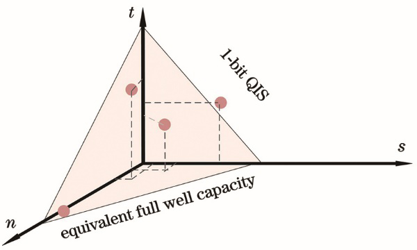
Fig. 1. Design space of QIS
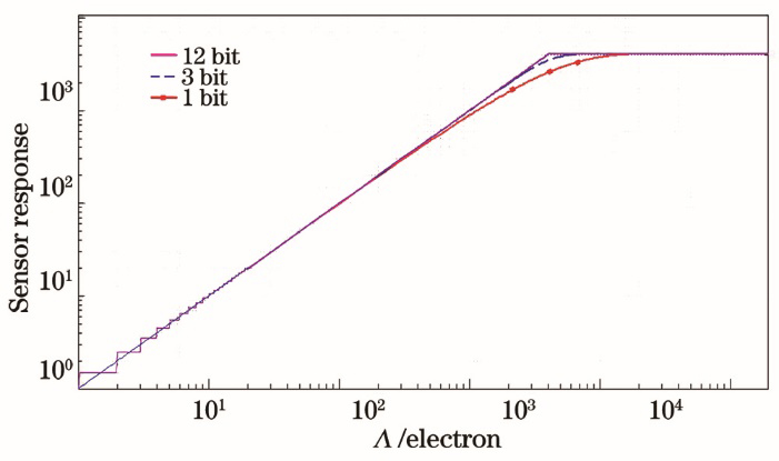
Fig. 2. Response curves under different bit-depths
Fig. 3. Influence of different sampling depth on dynamic range
Fig. 4. QIS imaging model
Fig. 5. PDF curve when k is 0 and 1
Fig. 6. EBR varing with read noise
Fig. 7. Photon counting error varing with read noise
Fig. 8. Photon counting error varing with λ
Fig. 9. Dynamic range and offset metric under different bit-depths
Fig. 10. ADC structure with gain stages
Fig. 11. Schematic diagram of 3-bit ADC circuit
Fig. 12. Working sequence diagram of 3-bit ADC
Fig. 13. Offset simulation results of ADC
Fig. 14. Power consumption of ADC
Fig. 15. Comparison of power consumption between traditional flash ADC and improved ADC
|
Table 1. Parameters involved in QIS imaging model

Set citation alerts for the article
Please enter your email address
© Copyright 2018-2021 | Chinese Laser Press. All Rights Reserved 沪ICP备15018463号-20