
Kai CAI, Zhiwen JIN. Photodetector Based on Two-dimensional Perovskite (PEA)2PbI4 [J]. Journal of Inorganic Materials, 2023, 38(9): 1069
- Journal of Inorganic Materials
- Vol. 38, Issue 9, 1069 (2023)
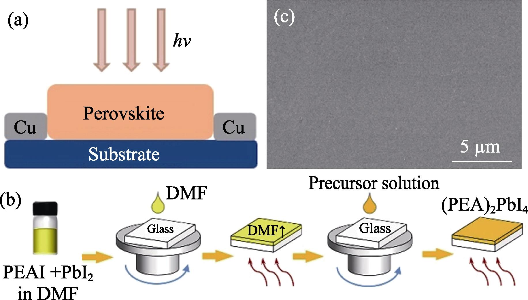
1. (a) Structure of the photodetector device prepared on a glass substrate, (b) schematic diagram of preparation process for the (PEA)2PbI4 thin film, and (c) SEM image of the (PEA)2PbI4 thin film after being annealed at 80 ℃

2. (a) XRD pattern of a typical (PEA)2PbI4 film,(b) crystal structure of two-dimensional layered (PEA)2PbI4, and (c) UV-Vis absorption and (d) PL spectra of (PEA)2PbI4 film
3. (a) Dark current versus applied voltage, (b) dark current versus time in the dark state, (c) I -V curves, and (d) I -t curves illuminated at different wavelengths with 1 mW/cm2 for (PEA)2PbI4 photodetector
4. (a) I -V and (b) I -t curves illuminated at 450 nm with different light intensities, (c) fitted line of photocurrent vs. light intensity illuminated at 450 nm, (d) responsivities and detectivities at different light intensities, (e) response time and (f) noise currents tested at different frequencies for (PEA)2PbI4 photodetector
5. Stability of the 2D (PEA)2PbI4 film and photodetector
S1. (a) Picture of a photodetector based on (PEA)2PbI4 film; (b) SEM image of (PEA)2PbI4 film after being annealed at high temperature(200 ℃)
S2. EDS mappings of (PEA)2PbI4 thin film
S3. XRD patterns of (PEA)2PbI4 without and with DMF treatment before spin-coating
S4. Tauc plot of (PEA)2PbI4 film with an optical band gap of 2.357 eV
S5. Bias-dependent photoconductivity of (PEA)2PbI4
S6. I-V curves of photodetector with up-electrode in the light-dark state


Set citation alerts for the article
Please enter your email address

© Copyright 2018-2021 | Chinese Laser Press. All Rights Reserved 沪ICP备15018463号-20