• Chinese Journal of Lasers
  • Vol. 46, Issue 10, 1001009 (2019)
Qinghe Yuan1、2, Hongqi Jing1、*, Li Zhong1, Suping Liu1, and Xiaoyu Ma1、2
Author Affiliations
  • 1National Engineering Research Center for Optoelectronic Devices, Institute of Semiconductors Chinese Academy of Sciences, Beijing 100083, China
  • 2College of Materials Science and Opto-Electronic Technology, University of Chinese Academy of Sciences,Beijing 100049, China
  • show less
    DOI: 10.3788/CJL201946.1001009 Cite this Article Set citation alerts
    Qinghe Yuan, Hongqi Jing, Li Zhong, Suping Liu, Xiaoyu Ma. Thermal Stressin High-Power Semiconductor Laser Packaging[J]. Chinese Journal of Lasers, 2019, 46(10): 1001009 Copy Citation Text show less
    Overall package structure of semiconductor laser bar
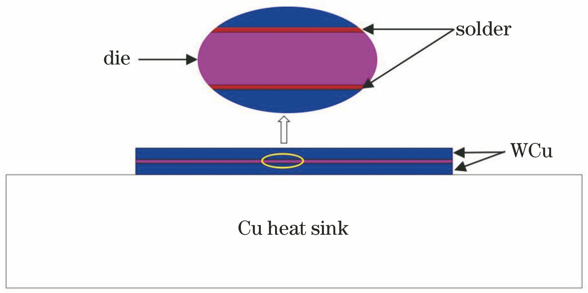
    Fig. 1. Overall package structure of semiconductor laser bar
    Nephograms of thermal stress distribution of laser dies with different solder packages and stress distributions on central axis of end face. (a) In solder, thermal stress nephogram; (b) In solder, stress distribution on central axis of end face; (c) AuSn solder, thermal stress nephogram; (d) AuSn solder, stress distribution on central axis of end face
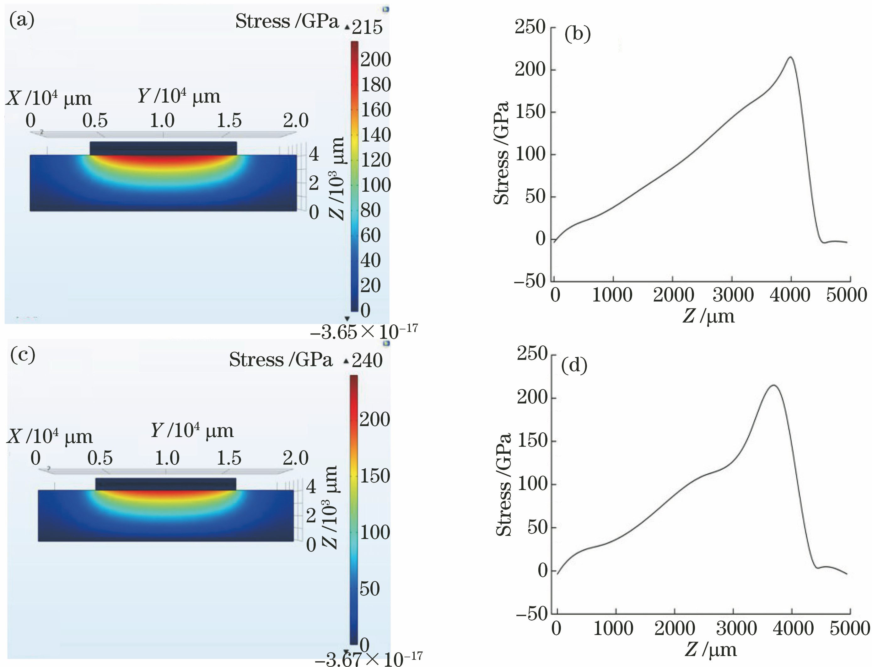
    Fig. 2. Nephograms of thermal stress distribution of laser dies with different solder packages and stress distributions on central axis of end face. (a) In solder, thermal stress nephogram; (b) In solder, stress distribution on central axis of end face; (c) AuSn solder, thermal stress nephogram; (d) AuSn solder, stress distribution on central axis of end face
    Temperature distributions of lasers with different solder packages. (a) In solder; (b) AuSn solder
    Fig. 3. Temperature distributions of lasers with different solder packages. (a) In solder; (b) AuSn solder
    Spectral distributions of lasers with different solder packages. (a) In solder; (b) AuSn solder
    Fig. 4. Spectral distributions of lasers with different solder packages. (a) In solder; (b) AuSn solder
    Thermal stress and temperature maximum distribution of laser dies packaged by AuSn solders with different thicknesses
    Fig. 5. Thermal stress and temperature maximum distribution of laser dies packaged by AuSn solders with different thicknesses
    Thermal stress and maximum temperature distribution of laser dies packaged by WCu submount with different thicknesses
    Fig. 6. Thermal stress and maximum temperature distribution of laser dies packaged by WCu submount with different thicknesses
    MaterialDensity /(kg·m-3)Coefficientof thermalexpansion /K-1Thermalconductivity /(W·m-1·K-1)PoissonratioYoung'smodulus /PaHeat capacity /(J·kg-1·K-1)Meltingpoint /℃
    Cu89002.4×10-53900.371.1×1011395-
    WCu170007×10-61800.33.4×1011750-
    In73103.3×10-581.60.44981.1×1010230156.61
    AuSn147001.6×10-5570.4056.8×1010150280
    GaAs53305.8×10-6440.258×109325-
    Table 1. Related material parameters
    Qinghe Yuan, Hongqi Jing, Li Zhong, Suping Liu, Xiaoyu Ma. Thermal Stressin High-Power Semiconductor Laser Packaging[J]. Chinese Journal of Lasers, 2019, 46(10): 1001009
    Download Citation