• Laser & Optoelectronics Progress
  • Vol. 57, Issue 9, 092002 (2020)
Ming Chang1, Rui Hu2, Yiping Wang1、*, Wei Xia1, and Yunjie Cheng1
Author Affiliations
  • 1School of Physical Science and Technology, Nanjing Normal University, Nanjing, Jiangsu 210023, China
  • 2Beijing Institute of Radio Measurement, Beijing 100854, China
  • show less
    DOI: 10.3788/LOP57.092002 Cite this Article Set citation alerts
    Ming Chang, Rui Hu, Yiping Wang, Wei Xia, Yunjie Cheng. Design and Research of A/D Sampling High-Speed Photoconductive Switch for Radio-Frequency Signal[J]. Laser & Optoelectronics Progress, 2020, 57(9): 092002 Copy Citation Text show less
    Structure diagram of photoconductive switch. (a) Schematic diagram; (b) physical map
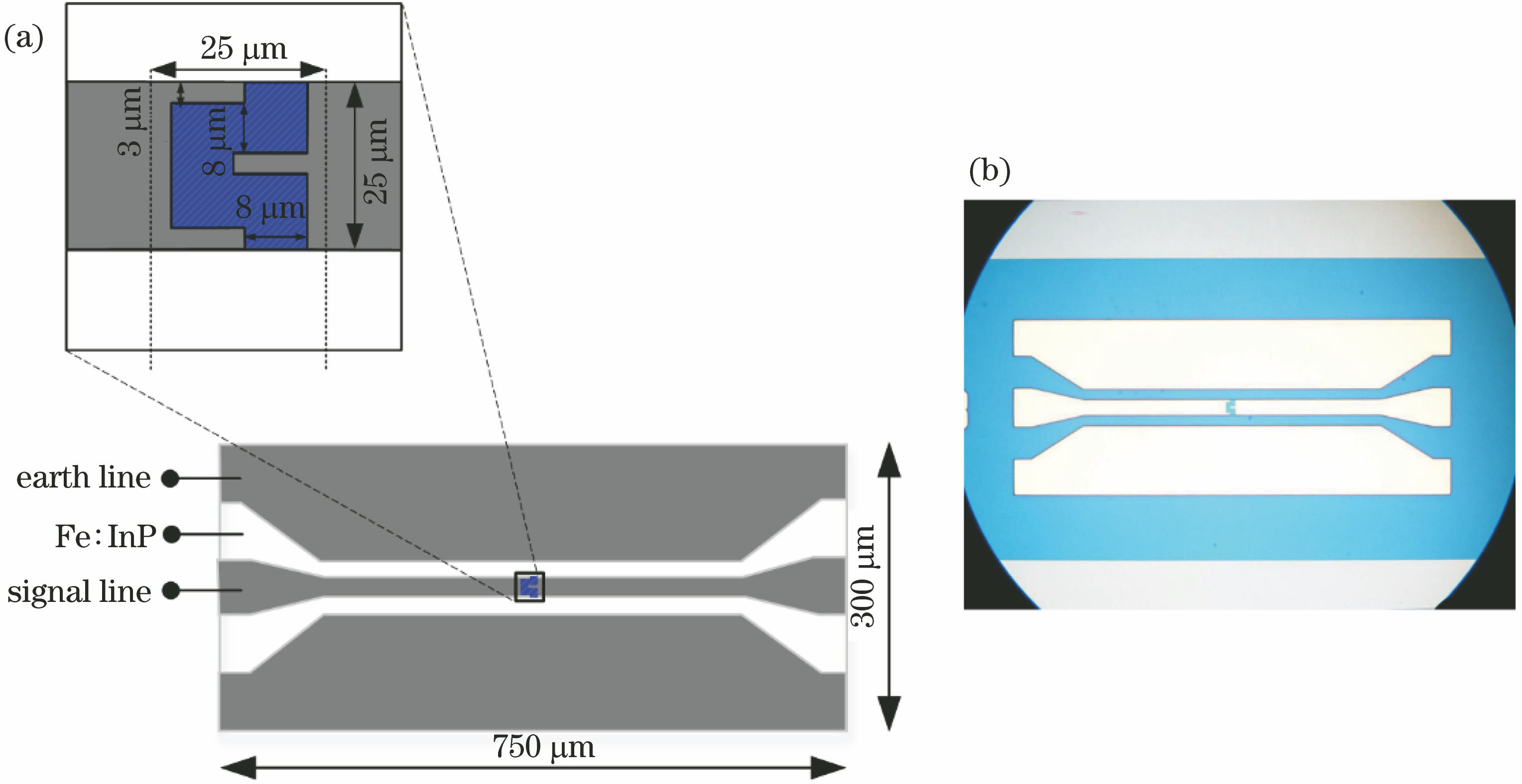
    Fig. 1. Structure diagram of photoconductive switch. (a) Schematic diagram; (b) physical map
    Lumped circuit model of photoconductive switch
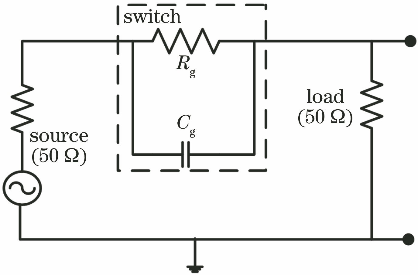
    Fig. 2. Lumped circuit model of photoconductive switch
    Principle of rectangular pulse sampling. (a) Time-domain waveform of signal to be sampled; (b) time-domain waveform of rectangular pulse sampling signal; (c) waveform multiplied in the time-domain of rectangular pulse sampling; (d) spectrum of the signal to be sampled; (e) spectrum of the sampled rectangular pulse signal; (f) spectrum of the final output signal after convolution in the frequency domain
    Fig. 3. Principle of rectangular pulse sampling. (a) Time-domain waveform of signal to be sampled; (b) time-domain waveform of rectangular pulse sampling signal; (c) waveform multiplied in the time-domain of rectangular pulse sampling; (d) spectrum of the signal to be sampled; (e) spectrum of the sampled rectangular pulse signal; (f) spectrum of the final output signal after convolution in the frequency domain
    Simulation results of switch S21 parameter
    Fig. 4. Simulation results of switch S21 parameter
    Schematic of RF signal transmission performance test
    Fig. 5. Schematic of RF signal transmission performance test
    Electrical transmission performance in dark and light. (a) Three interdigital electrodes; (b) two interdigital electrodes
    Fig. 6. Electrical transmission performance in dark and light. (a) Three interdigital electrodes; (b) two interdigital electrodes
    Effect of input optical power on on-off ratio
    Fig. 7. Effect of input optical power on on-off ratio
    Experimental photoconductive sampling system
    Fig. 8. Experimental photoconductive sampling system
    Spectrum after sampling. (a) Raw chip; (b) chip with nitrogen ion implantation
    Fig. 9. Spectrum after sampling. (a) Raw chip; (b) chip with nitrogen ion implantation
    Nyquist interval12345678Main spectrum
    Simulation /MHz32.283.8135.4187238.6290.2341.8393.4445
    Measurement /MHz32.171.1135.1174.1238.1278.1342.1381.1445
    Table 1. Theoretical and measured values of the mapping frequency of different Nyquist intervals
    Current /mA050100150200250300350400450500550600
    Main spectrum /dB0-4.84-2.91-1.94-1.28-0.62-0.57-0.41-0.33-0.30-0.20-0.08-0.01
    First Nyquistinterval /dB0-41.8-40.7-40.3-33.2-25.9-25.2-24.8-24.5-24.3-23.9-23.7-23.3
    Table 2. Input optical power corresponds to output spectral amplitude
    Ming Chang, Rui Hu, Yiping Wang, Wei Xia, Yunjie Cheng. Design and Research of A/D Sampling High-Speed Photoconductive Switch for Radio-Frequency Signal[J]. Laser & Optoelectronics Progress, 2020, 57(9): 092002
    Download Citation