1State Key Laboratory of Integrated Optoelectronics, College of Electronic Science and Engineering, Jilin University, Changchun 130012, China
2State Key Laboratory of Precision Measurement Technology and Instruments, Department of Precision Instrument, Tsinghua University, Beijing 100084, China
Femtosecond laser direct writing (FsLDW) three-dimensional (3D) photonic integrated circuits (PICs) can realize arbitrary arrangement of waveguide arrays and coupling devices. Thus, they are capable of directly constructing arbitrary Hamiltonians and performing specific computing tasks crucial in quantum simulation and computation. However, the propagation constant is limited to a narrow range in single-mode waveguides by solely changing the processing parameters, which greatly hinders the design of FsLDW PICs. This study proposes a composite waveguide (CWG) method to increase the range of , where a new single-mode composite waveguide comprises two adjacent circular waveguides. As a result, the photon propagation can be controlled and the variation range of can be efficiently enlarged by approximately two times (). With the CWG method, we successfully realize the most compact FsLDW directional couplers with a 9 μm pitch in a straight-line form and achieve the reconstruction of the Hamiltonian of a Hermitian array. Thus, the study represents a step further toward the fine control of the coupling between waveguides and compact integration of FsLDW PICs.
1. INTRODUCTION
Femtosecond laser direct writing (FsLDW) promotes the integration of photonic integrated circuits (PICs) from 2D into 3D by enabling arbitrary waveguide arrangement in three-dimensional (3D) space. Thus, FsLDW provides a straightforward solution to improve chip integration and a new physical degree of freedom to design and realize more complex on-chip photonic manipulation [1–7]. Moreover, FsLDW provides large amounts of technical support, especially in the emerging fields of quantum computing [8–12] and topological photonics [13–17] by adding refractive index and coupling modulation along the 3D waveguides. The 3D chip layouts were used to avoid waveguide crossings and realize oscillating potential so that the first on-chip photonic quantum Toffoli gate [12] and Floquet topological insulator [14] were exhibited.
In FsLDW-3D-PICs, the propagation constant () of waveguides relates to the effective refractive index () and represents the phase change of light per unit propagation length, which is crucial for both compact integration and quantum simulating. On the one hand, the higher the , the smaller the size of the waveguide devices. The realization of a high refractive index was strongly related to the type of glasses. Currently, the record high refractive index change for FsLDW waveguides is in fused silica, improving the integration of FsLDW PICs further [18]. On the other hand, the diagonal elements of the Hamiltonian matrix of a Hermitian system are generally filled with of each waveguide. By constructing a Hamiltonian with a waveguide array, some quantum mechanics states and dynamic processes, challenging or impossible to observe directly, can be equivalently mapped onto optical systems due to the formal unity of Schrödinger’s equation and light wave evolution equation in the waveguide array [19]. During the past decades, plenty of quantum phenomena have been observed through optical and quantum simulation, including Bloch oscillations [20,21], Anderson localizations [22], Zener tunneling [23], and gravitational lensing effect [24], proving it a strong and versatile tool for visualizing some quantum phenomena.
As the demands for integration of PICs and the simulated system complexity have increased, efforts have been devoted to obtaining a larger variation range of single-mode waveguides in FsLDW PICs. However, the methods to vary are either by inducing periodic bending waveguides [20,21] or changing the writing parameters, such as the writing velocity and pulse energy [25], which is not compact and induces a lower () than that of silicon waveguides. These methods lead to a larger evolution length for quantum simulators [26] and a larger size of waveguide devices [27]. Cheng et al. increased the of FsLDW bending waveguides by inducing bend–loss–suppression walls (BLSWs) [28]. However, the additional structure will limit the device design in large-scale PICs. Thus, developing a simple and controllable method to enlarge the through and finely regulate it is required to exploit the potentialities of 3D-FsLDW waveguide devices completely.
Sign up for Photonics Research TOC. Get the latest issue of Photonics Research delivered right to you!Sign up now
This paper presents a simple and efficient composite waveguide (CWG) method based on FsLDW technology to realize large propagation constant variation regardless of the type of glasses ( in Corning Eagle XG). The method enables the fine control of coupling and Hamiltonian reconstruction of waveguide arrays. A certain amount of propagation constant difference is induced by regulating the central distance between two circular sub-waveguides. The maximum of this varying amount is times higher () than that of varying the writing velocity (). Additionally, based on the CWG method, a novel and compact straight-line directional coupler (SL-DC) is proposed and optimized. The pitch of the SL-DC is successfully minimized to 9 μm. Finally, with the CWG method, the Hamiltonian reconstruction of a waveguide array is theoretically and experimentally studied. The control of crosstalk between different layers is simultaneously shown visually. The CWG method we demonstrate is a useful tool to realize coupling control between waveguides in 3D scales, which will promote the development of 3D integrated devices and quantum simulation.
2. COMPOSITE WAVEGUIDE METHOD
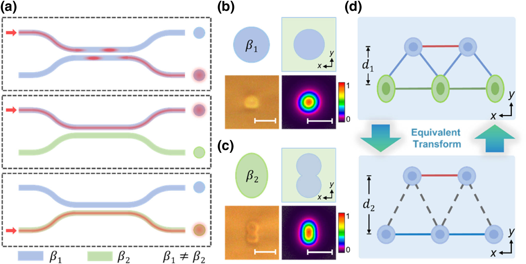
Jin et al. [29] proposed a double-track approach to deal with single waveguides (SWGs) restricted in terms of birefringence and mode-field shape. The approach has been widely applied to fine-regulate the birefringence of waveguides [30,31]. Nevertheless, the core idea of the proposed CWG method is to use two circular-cross section waveguides to construct a CWG with an elliptical mode profile to improve the control of the of the waveguide. As illustrated in Fig. 1(a), the injected light oscillates at the coupling region of a symmetric directional coupler (DC), and the energy is fully coupled from the input waveguide to the adjacent waveguide at the coupling lengths only if two waveguides have the same . While greatly differs from , the energy can be completely limited in the input waveguide, and the evanescent coupling between two waveguides can be further controlled. Here, the central distance of two sub-waveguides arranged in the vertical () direction is fine-regulated to introduce a certain between the CWG in Fig. 1(c) and the SWG in Fig. 1(b) (the basic information of the single circular waveguide, the optical microscope images of cross-sections, and mode profiles of CWGs with different central distances are provided in Appendix A). By implementing CWGs in some lattice sites of the waveguide array, as illustrated in Fig. 1(d), the coupling between different layers is suppressed, even at a normal coupling distance due to the high , as if these two layers are distant. This approach leads to an equivalent transformation on the array arrangement and, hence, its Hamiltonian.
Figure 1.Schematic of the CWG method. (a) Coupling control between two waveguides by varying the of waveguides. (b) and (c) are schematic and optical microscope photos of the waveguide cross-section and mode profiles of the SWG and CWG, respectively. (d) Schematic of equivalent transformation of the array Hamiltonian by placing CWGs in it. The scale bars in (b) and (c) are 10 μm.
Combining the FsLDW with a high-precision 3D linear stage (see Section 5 for fabrication details), the central distance between two sub-waveguides can be fine-regulated. A series of DCs, consisting of CWGs with varying central distance and SWGs, were fabricated with an interaction distance of 10 μm. As shown in Fig. 2(a), all transmissions of DCs with a certain CWG central distance are sine-squared. As the central distance increases, the maximum transmission of the oscillation curves decreases from to in Fig. 2(b), showing a significant negative correlation between the maximum transmissions and the central distance. The transmission of light in the coupling region of DCs can be described by the coupled mode theory (CMT) using Eqs. (1) and (2) as follows: where is the coupling coefficient. In addition, and denote the interaction length and the initial phase induced by arc-bending waveguides near the coupling region, respectively. Hence, can be obtained from the transmission curves in Fig. 2(a) using Eqs. (1) and (2). Figure 2(c) shows that increases nearly linearly with the central distance. Based on maintaining the CWGs single-mode, the maximum central distance reaches 3.6 μm under a writing velocity of 40 mm/s and induces a of . This value is times higher than those obtained by solely changing the writing velocity of SWGs under the same pulse energy (the pulse energy of a single circular waveguide is 390 nJ; see Section 5). This result indicates the feasibility of the method to expand the variation range of while being assisted with the change of velocity and single-pulse energy. Figure 2(d) exhibits the crosstalk between the 3.6 μm central-distance CWGs and SWGs of different waveguide distances (). As the increases from 9.5 to 12.5 μm, the crosstalk decreases from to a negligible , demonstrating a good anti-coupling effect (the mode profile images under different interaction lengths when CWGs are placed near SWGs are provided in Appendix A). This result implies that the 3.6 μm central-distance CWGs (all CWGs described in the following text correspond to the 3.6 μm central distance) can be used in 3D PICs to prevent optical signal crosstalk.
Figure 2.Characterization of the coupling properties between SWGs and CWGs. (a) Transmission of DCs composed of SWG and CWG with different central distances, and (b) the corresponding maximum transmission. (c) Propagation constant difference () between the SWG of 40 mm/s writing velocity and the other waveguides, including SWGs with different writing velocities and CWGs with different central distances. (d) Crosstalk between SWGs and 3.6 μm central distance CWGs under 808 nm testing laser.
Note that excessive loss to the original circuits by CWGs must be avoided to exploit the CWGs in PICs to control the evolution of the light wave. Here, the propagation loss of CWGs and mode-mismatch loss between CWGs and SWGs were studied. At first, the propagation loss of the CWGs is accurately measured to be 0.264 dB/cm using the method introduced in Ref. [32]. Then, by inserting a different number of CWG segments into a single SWG, as illustrated in the insets of Fig. 3(a), the total propagation loss (TPL) through the entire waveguide is given as follows: where , , and are the propagation loss of CWGs, SWGs, and the mode-mismatch loss between CWGs and SWGs, respectively. Additionally, , , and are the number of segments of CWGs, the length of a single CWG segment, and the total length of all waveguides. As is designed to be 3 mm, and can be obtained from the intercept and slope of the curve in Fig. 3(a), which is 0.273 dB/cm and 0.193 dB/facet, respectively. Note that the propagation losses of SWGs and CWGs are similar; however, the mode-mismatch loss is high, which is the main factor reducing the practical use of CWGs.
Figure 3.Loss characterization of CWG. (a) Propagation loss of CWG. (b) Mode-mismatch loss between the CWG and the SWG with different lengths of taper.
Furthermore, a designed taper was added between the CWG and the SWG to reduce the mode-mismatch loss between CWGs and SWGs. Before the taper, the SWG (or CWG) consisted of two single circular waveguides. Then, two circular waveguides were apart from each other (or merged together) in the direction to form the taper. As Fig. 3(b) shows, the mode-mismatch loss decreases while the length of the taper waveguide increases. With a taper length of 1.5 mm, the mode-mismatch loss is negligible, approximately 0.04 dB/facet. This result indicates that no excessive loss is introduced with the taper waveguides, and the CWGs with taper waveguides can be directly implanted in the PICs to manipulate the evolution of the light wave effectively.
C. SL-DCs
The conventional DCs comprise three parts: in/output ports, S bends, and coupling region. Only when two waveguides are close enough can the evanescent fields of two waveguides overlap, leading to the energy exchange between them. At the top of Fig. 4(a), S bends are generally designed to avoid the evanescent wave coupling effect outside the coupling region, which needs to separate the input and output ports to at least 24 μm in FsLDW PICs, resulting in chip space waste. Although two parallel straight waveguides of small interaction distance can also demonstrate coupling effects, the exchange of energy exists as long as the two waveguides are not separated. Because the CWGs do not couple with SWGs for high , the S bends can be equivalently replaced by CWGs, as illustrated at the bottom of Fig. 4(a), which minimizes the pitch between two ports of DCs in the direction to that size of the coupling region. Specifically, the CWGs and SWGs are connected by taper waveguides in Fig. 4(b) to lower the mode-mismatch losses. We set to 1.5 mm and the central distance, , to 3.6 μm. As the CWG approaches the SWG, the sectional optical microscope images in Fig. 4(b) suggest that the CWG adiabatically turns into the SWG. Subsequently, the transmission of SL-DCs with different coupling distances was studied with the vertically polarized (V polarization) laser injected through the SWG port [more detailed characterization of the transmission of SL-DCs under V and horizontal (H) polarization is given in Appendix B]. As the coupling distance varies from 9 to 12 μm, the coupling coefficient () ranges from 7.59 to . The sine-squared transmission in Fig. 4(c) indicates that the SL-DCs can perform the coupling function similar to the traditional DCs but with only one-third of the space. Compared with other FsLDW DCs [32–35], the SL-DCs are the shortest input/output pitch. Moreover, the results are significant in at least two major respects. First, waveguide devices comprising traditional DCs, such as MZIs, CNOT gates, and even 3D tritters, can be realized in a form containing straight waveguides, offering a new geometric design to waveguide devices. Second, by exploiting this design, the integration of PICs based on FsLDW technology can be improved.
Figure 4.SL-DCs. (a) Schematic of traditional DCs and SL-DCs. (b) Schematic of CWG port of the SL-DC. The CWG of the transmission area and the SWG of the coupling area were connected through taper waveguides. The insets in (b) correspond to the cross-section images of the CWG port; all scale bars are 10 μm. (c) The V polarization transmission of SL-DC with SWG port input while the interaction distance ranges from 9 to 12 μm.
The values of and of each waveguide are determined after the fabrication of the waveguide array. Thus, its Hamiltonian is determined under linear light. In particular, the only way to transform the Hamiltonian of an established array is to inject nonlinear light. This study demonstrated the Hamiltonian reconstruction of a waveguide array under linear light by applying the CWG method.
First, two 3D straight waveguide arrays were proposed, of which the schematics are shown in Figs. 5(a) and 5(b). One comprised SWGs, as illustrated in Fig. 5(c), while the SWGs at a deeper layer were precisely substituted by CWGs in the other array, as shown in Fig. 5(d). Two arrays, named SWG array and composite array, were fabricated; the cross-section microscope images are shown in Figs. 5(e) and 5(f). Because of the depth difference between these two layers, in the SWG array, the of the shallower layer was experimentally determined as higher than that of the deeper layer . In contrast, the diagonal coupling coefficient was lower than .
Figure 5.SWG waveguide arrays and composite arrays. (a), (b) 3D schematics of the proposed waveguide arrays. (c), (d) Pictorial representation of the cross-section of the SWG array and the composite array. to were arranged in a trapezoidal form at the plane. to and are the coupling coefficients between different waveguides, while is the gap between two layers. (e), (f) Corresponding optical microscope images of the cross-section regions of the SWG array and the composite array, respectively. The scale bars in (e) and (f) are 10 μm.
The normalized intensity of each waveguide in the array with different inputs can be obtained using the CMT (details in Appendix C). The optical axis of all waveguides is vertical (in the direction), which means that the light evolution for the H and V polarizations in the two arrays was basically the same except for the oscillation periods. Here, the experimental results of V polarization were considered for demonstration purposes. In particular, the laser was coupled into waveguides and of each array. Figures 6(a) and 6(b) show that as the laser is injected through and , respectively, the experimental data points at different propagation distances agree well with the theory results, represented by lines. Additionally, the experimental cross-sectional mode profile images at the propagation distances of 3, 5, and 7 mm are given in Fig. 6(c). Note that the laser energy can be close to fully coupled from the input ( or ) to other waveguides in the SWG array due to the negligible between SWGs. The light evolution in this SWG array was controlled and determined solely through a particular Hamiltonian. In the composite array, the corresponding Hamiltonian can be given as follows: where , , and are 3.3, 3.1, and , respectively. Although the non-zero , the coupling between CWGs and SWGs is negligible due to the high . Hence, can be replaced by 0, and is equivalent to
Figure 6.Hamiltonian reconstruction through the CWG method. (a), (b) Theoretical and experimental normalized intensity of different waveguides when the laser was injected into and of the SWG array. The theoretical results correspond to the lines in (a) and (b). (c) Experimental cross-section mode profile images at propagation distances of 3, 5, and 7 mm with and input. (d), (e) Theoretical and experimental normalized intensity of different waveguides when the laser was injected into and , respectively, of the composite array. Theoretical results correspond to the lines in (d) and (e). (f) Experimental cross-section mode profile images at propagation distances of 1, 5, and 9 mm with and input. The scale bars in (c) and (f) are 10 μm.
While linear light was injected into and of the composite array, the experimental normalized intensity of different waveguides was measured. The results are shown in Figs. 6(d) and 6(e). Simultaneously, the theoretical evolution of the light wave under the equivalent Hamiltonian is depicted as colored lines in Figs. 6(d) and 6(e). The experimental cross-section mode-profile images at 1, 5, and 9 mm propagation distances under fit well with the theoretical results of . This result indicates that the array of can govern the evolution of light wave as same as that of without a large to minimize (the equivalent SWG array demonstrating the same evolution of light is provided in Appendix C). Under the linear light propagation, the Hamiltonian of the composite array can be written as or , implying that the reconstruction of a waveguide array was realized. Furthermore, a comparison of the results in Figs. 6(c)–6(f) shows that the light propagating in one layer will not interfere with another layer with the CWG method, which is practical to control the crosstalk among the waveguides at different layers in the large-scale 3D PICs and increase integration.
4. CONCLUSION
In summary, we proposed a flexible CWG method based on FsLDW technology to induce a controllable amount of between the normal SWGs and the CWGs by regulating the central distance of two circular sub-waveguides. The maximum achieved by the CWG method is approximately twice that achieved solely by regulating the scanning velocity under the same processing power. Thus, the proposed method provides a new degree of freedom to enlarge regardless of the types of glasses. The measured propagation loss of CWGs and SWGs was as low as , while the mode-mismatch loss between each other was minimized to 0.02 dB/facet with the taper waveguides. By exploiting CWGs in the SWGs, the most compact FsLDW DC, the SL-DC, was demonstrated and investigated at interaction distances of 9 to 12 μm, exhibiting the same functions as traditional DCs with S bends while having a more integrated arrangement in the chip. The developed straight-line coupling devices provide insights that can help develop integrated waveguide devices such as SL-MZIs and SL-CONT gates. Moreover, Hamiltonian reconstruction under linear light was achieved by replacing some of the SWGs in an array with CWGs without the geometric changes in the arrangement of arrays.
This study demonstrated the full ability and relevancy of the CWG method in coupling control and Hamiltonian reconstruction. In particular, the CWG method could regulate the coupling ability between waveguides and promote the increased integration of 3D PICs. Moreover, the larger benefits the construction of a more complicated Hamiltonian, thereby simulating a more complicated physical system and observing the quantum dynamics in the optical system. In the future, by combining the 3D processing ability and the CWG method, the FsLDW PICs can open new ways to photonic simulations and integrated optics.
5. METHODS
Sample Fabrication. At first, the femtosecond (fs) laser pulses used in this study were generated by a commercial integrated fs-laser system (CARBIDE, Light Conversion Ltd.). The central wavelength, duration, and repetition rate of the pulses were 1030 nm, 290 fs, and 1 MHz, respectively. The fs laser pulses were focused by an objective lens (, , ; UPlanFL N, Olympus). The circular sub-waveguides were fabricated inside the borosilicate glass samples (EAGLE XG, Corning) with a pulse energy of 390 nJ and a writing velocity of 40 mm/s. The geometric center of all waveguide structures [including the structures in Figs. 1(b), 1(c), Figs. 2(b)–2(d), Fig. 3, Figs. 4(b), 4(c), Figs. 5(a)–5(c) and Figs. 6(a)–6(c)] were set at a depth of 190 μm beneath the surface of the substrates. The writing tracks were controlled accurately using an air-bearing X–Y–Z linear stage (ABL1000, Aerotech Inc., USA). Subsequently, the cross-sections of the fabricated photonic chips were finely polished for characterization using an automatic precision polishing machine (UNIPOL-802, Shenyang Kejing Auto-instrument Co., Ltd.).
Experimental Measurement. The laser was launched with a wavelength of 808 nm (MDL-III-808L, Changchun New Industries Optoelectronics Tech, Co., Ltd.) and butt-coupled into the waveguides through an objective lens (, , ). The polarization orientation of the light was controlled by combining a polarization beam splitter and a rotatable half-wave plate. A similar metallurgical objective was used to collect the light emitted from the waveguide cross-section. Subsequently, the power of the emitted laser and mode profiles were measured using a power meter (PM100D, Thorlabs Inc.) and a laser beam analyzer (SP928, Spiricon Inc.), respectively.
APPENDIX A: CHARACTERIZATION OF CWGs
CWGs with different central distances were characterized to find the largest central distance and ensure single-mode CWGs. Both the SWGs and CWGs are composed of two circular waveguides, while the central distance of two circular waveguides for SWGs is 0 μm. As shown in Figs. 7(a) and 7(f), the cross-section and mode profile diameter of the single circular waveguide are 3.9 μm and 4.4 μm, respectively. The effective refractive index for SWGs in Fig. 7(b) is determined to be . Furthermore, the CWGs in Figs. 7(b)–7(e) are all single-mode, and the mode profiles become oblong with the increase in the central distance. The sub-waveguides of CWGs turn into two independent waveguides when the central distance exceeds 3.6 μm.
Figure 7.Characterization of cross-section morphology and mode properties of waveguides. Optical microscope images (a)–(e) and mode-profile images (f)–(j) of the cross-section of the single circular waveguide and waveguides with central distances of 0, 1.2, 2.4, and 3.6 μm, respectively. Scale bars in all images are 5 μm.
Figure 8.Characterization of the coupling regions with different interaction lengths. (a1)–(a3) Energy distribution of two SWGs with an interaction distance of 10 μm. Energy distribution of the combination of an SWG and a 3.6 μm central-distance CWG when the laser was injected through (b1)–(b3) CWGs and (c1)–(c3) SWGs, respectively. Scale bars in all images are 5 μm.
The light was coupled into the CWG port to fully characterize the coupling ability of SL-DCs in Fig. 4. The transmissions are shown in Fig. 9(a). The experimental data agree with the fitting curves, demonstrating a good coupling function with both input ports. In addition, the comparison of the output profiles images in Figs. 9(b)–9(g) with Figs. 8(b1)–8(c3) shows that the evanescent wave coupling effect occurs in the straight-line DCs because the light is present in both CWGs and SWGs under the interaction of 9 μm.
Figure 9.(a) Transmission of SL-DC injected with the V polarization laser through the CWG port while the interaction distance ranges from 9 to 12 μm. Experimental cross-section modal profiles of SL-DCs with 9 μm interaction distance while being injected with the SWG port (b)–(d) and the CWG port (e)–(g). The injected light could be nearly fully coupled from the injected port to the adjacent port. Scale bars in (b)–(g) are all 5 μm.
APPENDIX C: NUMERICAL CALCULATION OF LIGHT EVOLUTION IN WAVEGUIDE ARRAYS
The numerical calculation of the light wave evolution in the SWG arrays and composite arrays is given in Fig. 11 based on CMT. For a waveguide array with straight waveguides, by numbering the waveguides in the array from 1 to , the Hamiltonian (with a dimension of ) of each array can be derived. Then, the output probability amplitude distribution (with a dimension of ) at the interaction length of can be given by where . and are the Kronecker delta and the vector of 1 (with a dimension of ), respectively [36]. is the input probability amplitude distribution of the waveguides. The relative output energy of the th waveguide at the length of can be written as
Figure 11.Calculated light wave evolution in the SWG array and composite array by the CMT. (a), (b) Theoretical evolution of light in the SWG array when injected through and , respectively. The insets are the calculated cross-sectional profiles at the propagation distance of 3, 5, and 7 mm. (c), (d) Theoretical evolution of light in the composite array when injected through and , respectively. The insets are the calculated cross-sectional profiles at the propagation distance of 1, 5, and 9 mm.
Figure 12.Corresponding equivalent SWG array of the composite array in Fig. 6. (a) Pictorial representation of the cross-section of the equivalent array. to were arranged in a trapezoidal form at the plane. (b) Optical microscope images of the composite array cross-section. The distance between the shallower layer and the deeper was 18 μm. (c) and (d), (e) and (f), and (g) and (h) are the experimental laser intensity distributions of the array cross-section under the propagation distance of 1, 5, and 9 mm when the laser was injected into and . The scale bars in (b)–(h) are 10 μm.