
Xin Wei, Weiwei Zhao, Jintao Yang, Yong Zhang, Junming Song, Zhenhua Ni, Junpeng Lu, Hongwei Liu. Direct writing-in and visualizing reading-out data storage with high capacity in low-cost plastics[J]. Journal of Semiconductors, 2022, 43(6): 062301
- Journal of Semiconductors
- Vol. 43, Issue 6, 062301 (2022)
Abstract
1. Introduction
With the rapid development of the digital era, information including character, sound, image and video is boosting faster than ever[
Here, optical data storage with a capacity of ~1 TB is realized in PMMA by means of fs laser writing. The high data capacity arises from the 3D storage schema and multiple gray levels of fluorescent contrast. By penetrating the interior of PMMA to achieve multilayer data writing, the focused laser beam enables 3D information storage. The superior linear correlation between the single pulse energy and fluorescent contrast renders the direct writing-in of 8 gray levels. Moreover, the written data present a low bit error rate, fast writing speed, direct visual reading and high stability. This optical data storage technique is expected to offer an implementable multidimensional light disk to match the requirement of rapidly growing data volumes.
2. Experimental section/methods
2.1. Materials and methods
Transparent PMMA (CQ grade, Goodfellow, UK), polycarbonate (PC), precipitated calcium carbonate (PCC) and polystyrene (PS) samples were purchased online. The femtosecond laser used was an amplified Ti:sapphire laser with a central wavelength of 800 nm, a pulse duration of 35 fs and a repetition rate of 1 kHz. An array of periodic laser-induced bits was fabricated through a homemade 3D three-dimensional laser processing system. To increase the storage density, we used a high NA 100× with a 1.2 mm working distance IR objective bought from Olympus. Moreover, the environmental parameters of the aging experiment were controlled by an industrial grade constant temperature and humidity chamber.
2.2. Characterization
The UV–vis absorption spectrum, PL spectra and confocal fluorescence microscope images were measured by using a Shimadzu UV/Vis UV‐2600 spectrometer, a WITEC-R200 and K1-Fluo RT, respectively. According to the depth of the laser-modified region, an oil immersion microscope objective (Olympus, UPlanSApo, 1.2 NA, 60× magnification, 0.28 mm working distance) and an air microscope objective (Olympus, UPlanSApo, 0.75 NA, 20× magnification, 0.6 mm working distance) for confocal fluorescence microscopy images were used to focus light to the region modified by the fs laser. The mean and standard deviation of laser-induced fluorescence that was read out by commercial confocal fluorescence microscopy and were evaluated using ImageJ software.
3. Results and discussion
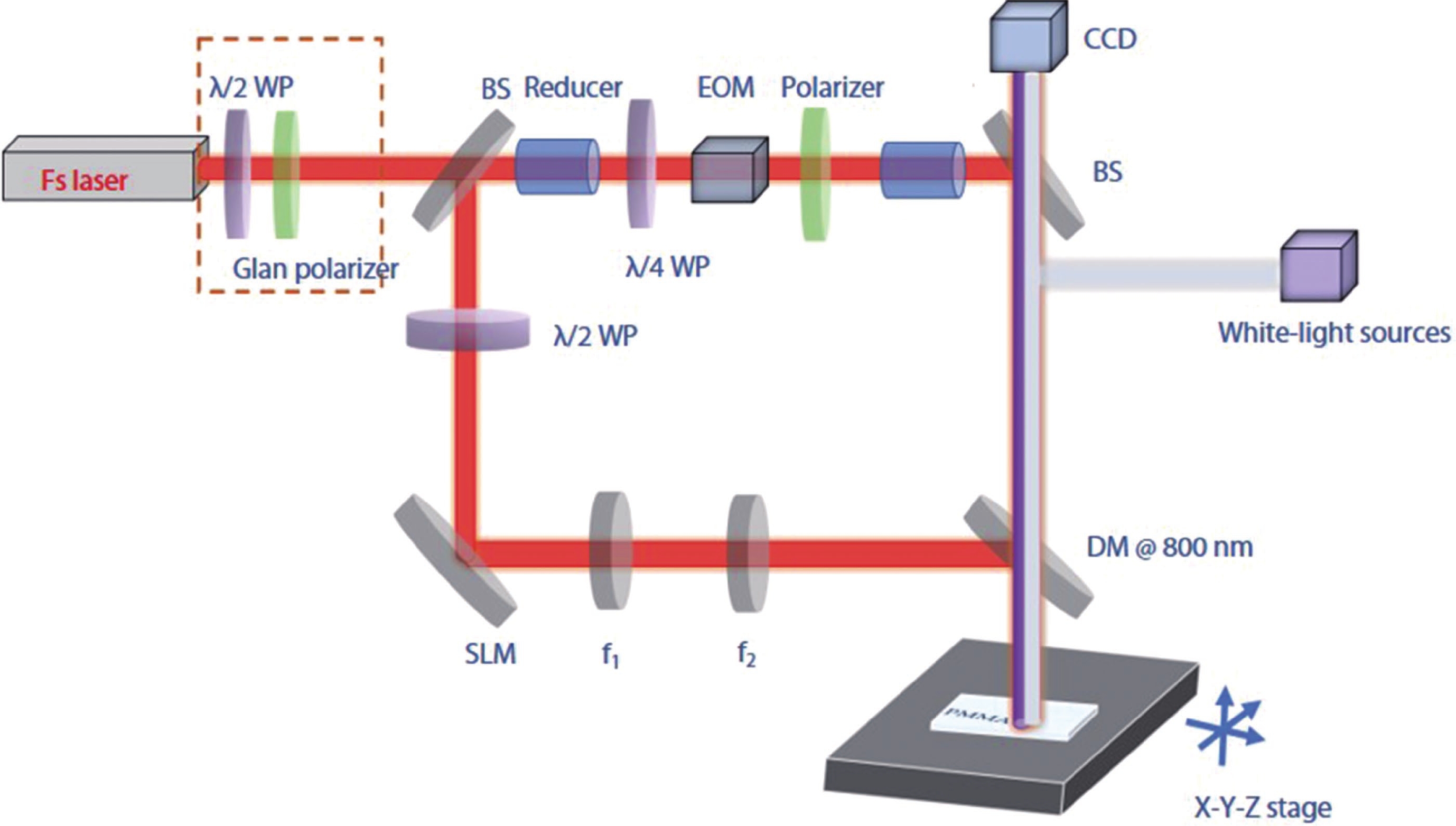
Fig. 1 and Fig. S1 present a sketch and actual scene of the ultrahigh-density 3D laser-based data storage platform. Here, we employed a 1 kHz, 800 nm Ti:sapphire oscillator–amplifier laser system as the light source, producing an ~3.5 mJ pulse with a laser peak width of ~35 fs. The fs laser can be controllably driven, modifying the microscale region in bulk materials or low-dimensional materials. To precisely and rapidly control the laser power, we introduce a combination of an electro-optic modulator (EOM), a quarter-wave plate and a polarizer. Moreover, we introduce a liquid crystal spatial light modulator associated with the 4f system for multibeam parallel processing[
![]()
Figure 1.(Color online) Schematic diagram of the femtosecond laser writing system.
Based on the self-developed laser writing system, various kinds of low-cost plastics, such as PC, PCC, PS and PMMA, which do not fluoresce in the visible spectrum before laser modification, can be considered candidates for optical storage research. Once the chosen regions of PC, PCC, PS and PMMA are irradiated by the laser, significant fluorescence is observed from the laser irradiated regions by confocal microscopy equipped with a reading laser wavelength of 405 nm and with a highly sensitive photomultiplier with a filter ranging from 420–750 nm (Fig. S2). The PL may originate from fs-laser-induced bond scission of plastics, which can serve as the fluorescence emission center[
![]()
Figure 2.(Color online) (a) PL spectra of pristine and laser-irradiated PMMA (single fs). The PL data were acquired using 355, 532 and 633 nm lasers. (b) SEM image of dots modified by threshold fs laser power at the surface. (c, d) Optical and confocal fluorescence microscopy images of the dots beneath the 30
For effective use of their interior space, modification should be attempted by focusing the beam into the interior of the low-cost plastics. PMMA was purchased from the Goodfellow company, the absorption spectrum of which is shown in Fig. 3(a). The high transmittance of transparent PMMA in the visible wavelength indicates that it is feasible to write information into the interior volume using a fs laser so that a slight pattern can be recorded at different depths of the low-cost transparent material by adjusting the z position of the laser focal plane. Via a fixed excitation energy, a uniform intensity of fluorescence can be written into each data layer. The fluorescence intensity can be assigned to the “on” or “off” state as the “0” and “1” states in traditional CDs or DVDs. The 3D confocal fluorescence microscope image shown in Fig. 2(b) further proved that 3D optical storage was successfully released based on the different layer writing. Based on photoinduced fluorescence, bit data or designed patterns, such as the Emblem of Nanjing Normal University and Southeast University, the Great Wall and Albert Einstein can be stored inside the bulk sample, as shown in Fig. 3(c) and Fig. S3.
![]()
Figure 3.(Color online) (a) Absorption spectrum of pristine PMMA, the chemical structure of which is shown in the inset. (b) The 3D fluorescence structure of the array with fixed writing power (40 nJ) inside PMMA separated by 10
By adjusting the power density of the focused laser, multiple gray levels can be assigned, further improving the data storage capacity. Modulating the pulse duration or pulse energy, the writing parameters could be used to achieve controllable fluorescence intensity[
![]()
Figure 4.(Color online) (a, c) Confocal fluorescence microscopy images of the dots (1st and 50th layers) written by a fs laser with a single pulse, scale bar: 20
The bit error rate in the optical disk is extremely important to realize industrial application[
![]()
Figure 5.(Color online) Gray level assignment based on fluorescence distinguish. It should be noted that both (a) the fresh sample and (b) the aged sample can be of capability of 8 gray level assignment.
4. Conclusion
In conclusion, we reported 3D optical memory in PMMA using the femtosecond pulsed laser processing platform. Multilayered bit patterns (bit resolution = 600 nm, layer separation =10 μm, gray levels = 8) can be recorded into the volume and can be conveniently read out through commercial confocal microscopes. The change in fluorescence intensity corresponding to the gray level of memory bits remained stable in extreme aging circumstances, which was essential for long-term preservation. This high storage optical disk can provide an innovative perception to advance optical data storage technology for information explosions.
Acknowledgements
This work was supported by the National KRDPC (2019YFA0308000, 2021YFA1200700), NSFC (91963130, 61927808, 62174026). The project is supported by “the Fundamental Research Funds for the Central Universities”.
Appendix A. Supplementary material
Supplementary materials to this article can be found online at https://doi.org/10.1088/1674-4926/43/6/062301.
References
[1] Q F Dai, O Y Min, W G Yuan et al. Encoding random hot spots of a volume gold nanorod assembly for ultralow energy memory. Adv Mater, 29, 1701918(2017).
[2] M Gu, Q Zhang, S Lamon. Nanomaterials for optical data storage. Nat Rev Mater, 1, 16070(2016).
[3] S Lin, H Lin, C Ma et al. High-security-level multi-dimensional optical storage medium: Nanostructured glass embedded with LiGa5O8:Mn2+ with photostimulated luminescence. Light Sci Appl, 9, 22(2020).
[4] A S van de Nes, J M Braat, S F Pereira. High-density optical data storage. Rep Prog Phys, 69, 2323(2006).
[5] S Kawata, Y Kawata. Three-dimensional optical data storage using photochromic materials. Chem Rev, 100, 1777(2000).
[6] B H Cumpston, S P Ananthavel, S Barlow et al. Two-photon polymerization initiators for three-dimensional optical data storage and microfabrication. Nature, 398, 51(1999).
[7] C Corredor, Z L Huang, K Belfield. Two-photon 3D optical data storage via fluorescence modulation of an efficient fluorene dye by a photochromic diarylethene. Adv Mater, 18, 2910(2006).
[8] Y Shen, J Swiatkiewicz, D Jakubczyk et al. High-density optical data storage with one-photon and two-photon near-field fluorescence microscopy. Appl Opt, 40, 938(2001).
[9] K D Belfield, K J Schafer. A new photosensitive polymeric material for WORM optical data storage using multichannel two-photon fluorescence readout. Chem Mater, 14, 3656(2002).
[10] G Kämpf, D Freitag, G Fengler et al. Polymers for electrical and optical data storage. Polym Adv Technol, 3, 169(1992).
[11] E Betzig, J K Trautman. Near-field optics: Microscopy, spectroscopy, and surface modification beyond the diffraction limit. Science, 257, 189(1992).
[12] Y L Hu, D Wu, J W Li et al. Two-stage optical recording: Photoinduced birefringence and surface-mediated bits storage in bisazo-containing copolymers towards ultrahigh data memory. Opt Express, 24, 23557(2016).
[13] X P Yuan, M Zhao, X J Guo et al. Ultra-high capacity for three-dimensional optical data storage inside transparent fluorescent tape. Opt Lett, 45, 1535(2020).
[14] H Sano, T Shima, M Kuwahara et al. Response function of super-resolution readout of an optical disc studied by coupled electromagnetic–thermal simulation. Jpn J Appl Phys, 55, 09SB02(2016).
[15] F X Zhai, F Y Zuo, H Huang et al. Optical switch formation in antimony super-resolution mask layers induced by picosecond laser pulses. Chin Phys Lett, 27, 014209(2010).
[16] L P Shi, T C Chong, X S Miao et al. A new structure of super-resolution near-field phase-change optical disk with a Sb2Te3 mask layer. Jpn J Appl Phys, 40, 1649(2001).
[17] Y Liu, Y Lu, X Yang et al. Amplified stimulated emission in upconversion nanoparticles for super-resolution nanoscopy. Nature, 543, 229(2017).
[18] P Zijlstra, J W M Chon, M Gu. Five-dimensional optical recording mediated by surface plasmons in gold nanorods. Nature, 459, 410(2009).
[19] X Fang, H Ren, M Gu. Orbital angular momentum holography for high-security encryption. Nat Photonics, 14, 102(2020).
[20] X Li, H Ren, X Chen et al. Athermally photoreduced graphene oxides for three-dimensional holographic images. Nat Commun, 6, 6984(2015).
[21] D Z Tan, X Y Sun, Q Wang et al. Fabricating low loss waveguides over a large depth in glass by temperature gradient assisted femtosecond laser writing. Opt Lett, 45, 3941(2020).
[22] Z Wang, D Z Tan, J R Qiu. Single-shot photon recording for three-dimensional memory with prospects of high capacity. Opt Lett, 45, 6274(2020).
[23] J W Chan, T R Huser, S H Risbud et al. Waveguide fabrication in phosphate glasses using femtosecond laser pulses. Appl Phys Lett, 82, 2371(2003).
[24] X J Huang, Q Y Guo, D D Yang et al. Reversible 3D laser printing of perovskite quantum dots inside a transparent medium. Nat Photonics, 14, 82(2020).
[25] H W Lee, M A Schmidt, P Uebel et al. Optofluidic refractive-index sensor in step-index fiber with parallel hollow micro-channel. Opt Express, 19, 8200(2011).
[26] K Miura, J R Qiu, S Fujiwara et al. Three-dimensional optical memory with rewriteable and ultrahigh density using the valence-state change of samarium ions. Appl Phys Lett, 80, 2263(2002).
[27] Z G Nie, H Lee, H Yoo et al. Multilayered optical bit memory with a high signal-to-noise ratio in fluorescent polymethylmethacrylate. Appl Phys Lett, 94, 111912(2009).
[28] P S Salter, M Baum, I Alexeev et al. Exploring the depth range for three-dimensional laser machining with aberration correction. Opt Express, 22, 17644(2014).
[29] B P Cumming, A Jesacher, M J Booth et al. Adaptive aberration compensation for three-dimensional micro-fabrication of photonic crystals in lithium niobate. Opt Express, 19, 9419(2011).
[30] Z Kuang, D Liu, W Perrie et al. Fast parallel diffractive multi-beam femtosecond laser surface micro-structuring. Appl Surf Sci, 255, 6582(2009).
[31] H Cheng, C Xia, S M Kuebler et al. Aberration correction for SLM-generated Bessel beams propagating through tilted interfaces. Opt Commun, 475, 126213(2020).
[32] M Hacker, G Stobrawa, R Sauerbrey et al. Micromirror SLM for femtosecond pulse shaping in the ultraviolet. Appl Phys B, 76, 711(2003).
[33] A M Alshehri, K L N Deepak, D T Marquez et al. Localized nanoclusters formation in PDMS upon irradiation with femtosecond laser. Opt Mater Express, 5, 858(2015).
[34] K Shibagaki, N Takada, K Sasaki et al. Synthetic characteristics of large carbon cluster ions by laser ablation of polymers in vacuum. J Appl Phys, 93, 655(2002).
[35] M Gu, X P Li. The Road to multi-dimensional bit-by-bit optical data storage. Opt Photonics News, 21, 28(2010).
[36] Z C Ma, Y L Zhang, B Han et al. Femtosecond-laser direct writing of metallic micro/nanostructures: From fabrication strategies to future applications. Small Methods, 2, 1700413(2018).
[37] K L N Deepak, R Kuladeep, S V Rao et al. Luminescent microstructures in bulk and thin films of PMMA, PDMS, PVA, and PS fabricated using femtosecond direct writing technique. Chem Phys Lett, 503, 57(2011).
[38] X J Huang, Q Y Guo, S L Kang et al. Three-dimensional laser-assisted patterning of blue-emissive metal halide perovskite nanocrystals inside a glass with switchable photoluminescence. ACS Nano, 14, 3150(2020).
[39] S Kawata, H B Sun, T Tanaka et al. Finer features for functional microdevices. Nature, 412, 697(2001).
[40] M Straub, M Gu. Near-infrared photonic crystals with higher-order bandgaps generated by two-photon photopolymerization. Opt Lett, 27, 1824(2002).
[41] A Jurado-Navas, J M G Balsells, J F Paris et al. General analytical expressions for the bit error rate of atmospheric optical communication systems. Opt Lett, 36, 4095(2011).
[42] I J Goldfarb, R J McHenry, E C Penski. Thermal degradation of polymers. I. Aspects of polytetrafluoroethylene degradation. J Polym Sci, 58, 1283(1962).


Set citation alerts for the article
Please enter your email address

© Copyright 2018-2021 | Chinese Laser Press. All Rights Reserved 沪ICP备15018463号-20