
Anton Rudenko, Maria K. Hagen, Jörg Hader, Stephan W. Koch, Jerome V. Moloney, "Self-consistent Maxwell–Bloch model for high-order harmonic generation in nanostructured semiconductors," Photonics Res. 10, 2099 (2022)
- Photonics Research
- Vol. 10, Issue 9, 2099 (2022)
Abstract
1. INTRODUCTION
All-dielectric nanostructured materials have been extensively applied to enhance and confine electric and magnetic fields at subwavelength scales for nonlinear optical applications [1–4]. Several strategies were proposed to increase the second- and third-order nonlinear conversion efficiency in semiconductors, based on Mie resonances in high-refractive-index nanostructures [5,6], as well as resonant metasurfaces [7–9]. Recently, a new paradigm of harmonic generation beyond the perturbative regime by strong field excitation has been demonstrated in semiconductors, opening new frontiers for previously non-accessible enhanced high-order harmonic spectra, consisting of odd and even harmonics and stretching far beyond third-order nonlinearities [10–15], and ultrafast all-optical modulation [16–19]. Comprehensive understanding of these coherent nonlinear excitation processes in semiconductors is still lacking, and self-consistent models are highly challenging due to the inclusion of the dynamical material response on a quantum level beyond the perturbative regime. Nonlinear conversion efficiency depends strongly on multiple involved phenomena such as intra-band and inter-band excitation dynamics [10,11,17], absorption induced by free carriers limiting the harmonics yield above the material bandgap [7] and shifting the nanostructure resonance positions [4,20], and nonlinear propagation effects [21,22].
The nature of odd and even harmonic generation in semiconductors has been established only recently, underlying the pronounced role of quantum interference and indirect transitions between valence and conduction bands [11,23,24]. The latter effects can be described by a quantum approach, as provided by semiconductor Bloch equations (SBEs) under inclusion of more than two mutually dipole coupled bands [25]. This momentum-resolved approach evaluates microscopic coherent carrier densities and polarizations within the non-equilibrium electronic system, considering the full Brillouin zone (BZ). Typically, a realistic model for the electronic band structure for a particular semiconductor is provided by density functional theory (DFT) simulations. In contrast to perturbative models, SBEs automatically include nonlinearities of any order as well as the full dynamic evolution of electronic material excitations. Furthermore, the non-perturbative nonlinearities were shown to play a significant role in off-resonant strong-field excitation and high-harmonic generation in semiconductors, attributed to dynamic intra-band oscillations that can be captured only by employing a dynamic microscopic model such as SBEs [26,27]. These non-perturbative scaling laws for high harmonics are influential in gallium arsenide (GaAs) for laser intensities of at least
To simulate the nonlinear spectrum evolution upon ultrashort laser pulse propagation through bulk material, the SBEs were further coupled to unidirectional or 1D/2D propagation codes by macroscopic polarization currents [22,28,29]. To date, only a few works have focused on the self-consistent coupling between full-vector Maxwell equations and SBEs [30–32], albeit not for harmonic generation. A 3D modeling is essential here not only to reproduce the exact geometry and resonant nature of the nanostructures, but also to take account the inhomogeneous distribution of laser-induced carriers [17,18,33,34].
Sign up for Photonics Research TOC. Get the latest issue of Photonics Research delivered right to you!Sign up now
In the current work, we demonstrate the feasibility and robustness of a coupled Maxwell–Bloch approach for investigating the high-order harmonic spectra for finite slab and 3D sub-wavelength nanoparticle geometries in the non-perturbative regime of ultrashort laser pulse excitation. Driven by either a Fabry–Perot-like standing wave resonator or magnetic dipole resonances, inhomogeneously photo-induced carriers are localized in the semiconductor material, producing enhanced even and odd harmonics.
2. NUMERICAL MODEL
The approach consists of two coupled parts: Maxwell equations with nonlinear polarization
A. Propagation
The propagation model is based on full-vector Maxwell equations with macroscopic currents to include linear dispersion and inter-band and intra-band excitation upon ultrashort pulse excitation as follows:
Throughout the paper, a linearly polarized plane wave excitation source is used. The electric field source is chosen to be an
B. Electronic Band Structure
Our GaAs band structure parameters are obtained via DFT assuming (111) crystal orientation. In our simulations, we include the mutually dipole coupled conduction
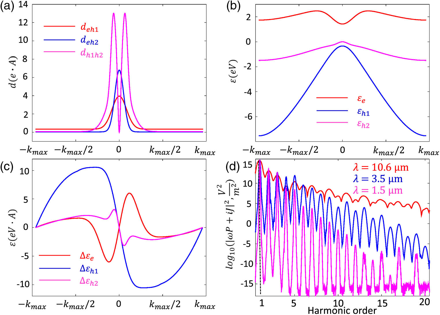
Figure 1.(a)–(c) Three-band structure for a non-centrosymmetric direct-gap semiconductor: GaAs (111) inspired (a) dipole coupling strength, (b) energies, and (c) their gradients. (d) High-harmonic spectra generated by an SBE model for
C. Semiconductor Bloch Equations
The macroscopic intra-band current and inter-band polarization are calculated through complex microscopic polarizations
To solve the SBEs, a fourth-order Runge–Kutta method is applied for the ensemble of microscopic polarizations
In the framework of the SBE model, the major changes in both real and imaginary refractive indices are considered via the complex intra-band and inter-band currents. Band-filling dynamics is included via the Pauli blocking factor
D. Coupling Maxwell Equations and SBEs
Our numerical method for the coupled Maxwell Eq. (1) and SBE Eq. (3) evaluates additionally the nonlinear electric field component
The field is sourced in vacuum at a distance from the nonlinear material. The time history of the electric field evolution is recorded in space positions before and after hitting the semiconductor material to obtain separate reflected and transmitted field signals, which are then further analyzed by Fourier transforms. A harmonic and decaying window function is applied at the boundaries of the temporal domain [35] to reduce the noise floor due to the finite size of the used Gaussian pulse and the accumulation effects related to the numerical dispersion.
3. RESULTS AND DISCUSSION
For our study, there are two specific regimes of interest for harmonic generation in semiconductor nanomaterials: a propagative regime in finite structures on the distances of order or larger than laser wavelength and a field confinement regime in subwavelength nanostructures, where the field can be significantly enhanced and the photo-generated carriers are localized inside the nanostructure.
A. Propagation in a Finite Slab: Fabry–Perot Resonances
First, we investigate the ultrashort laser pulse propagation through finite slabs of different thicknesses, effectively representing examples of a Fabry–Perot resonator due to the refractive index differences between vacuum and semiconductor material. Light waves entering the slab, being smaller than the optical pulse length
The spatiotemporal evolution of the electric fields for slab thicknesses of 12 and 24 μm is shown in Figs. 2(a) and 2(c) with the laser pulse propagating from down upwards. We see that for the thicker slab, the first and secondary reflection signals are separated in time, whereas for the thinner slab, they overlap. The maximum electron density distributions established at the end of the pulse are detailed in Figs. 2(b) and 2(d), representing periodic concentrated regions of increased charge carriers spaced by
![]()
Figure 2.Spatiotemporal evolution of (a), (c) electric fields, (b), (d) averaged carrier densities inside the slab of (a), (b) 12 μm and (c), (d) 24 μm thicknesses. Laser irradiation parameters are
In Fig. 3(a), we show spectra of the transmitted fields as a function of the propagation distance in comparison to the local emission spectrum
![]()
Figure 3.(a) Transmission spectra (solid lines) upon propagation on distances of compared to the emission spectra from point SBE model (dashed line). Comparison of transmission (red) and reflection (blue) spectra for slabs of (b) 12 μm and (c) 48 μm thickness; temporal evolution of the corresponding electric fields for (d) 12 μm and (e) 48 μm slabs. Incident pulses are marked by yellow boxes. Laser irradiation parameters are
Reflection and transmission spectra are compared for 12 and 48 μm slabs in Figs. 3(b)–3(e) [Fourier transforms in Figs. 3(b) and 3(c), and corresponding temporal signals in Figs. 3(d) and 3(e)].
B. Subwavelength Nanoparticle: Excitation of Mie Resonances
Nonlinear field effects can be significantly enhanced in subwavelength nanostructures of high-refractive-index materials supporting Mie resonances. We investigate here the ultrashort laser pulse excitation of a single spherical GaAs-like nanoparticle at
Extinction cross sections as a function of the nanoparticle radii at 1.5 μm wavelength are calculated by Mie theory [40] and plotted in Fig. 4(a). The sizes of choice are marked by colored points, corresponding to different positions respective to a magnetic dipole resonance (“MD” in the figure) and contrasting electric field distributions inside the nanoparticles. The intensities corresponding to an incident field
![]()
Figure 4.(a) Extinction cross section for GaAs nanoparticles of different radii. Magnetic dipole (MD), electric dipole (ED), and magnetic qudrupole (MQ) resonances are indicated. (b) 1D conduction band densities
Figures 5(a) and 5(b) show the computed transmission and reflection spectra for nanoparticles of different radii, indicating the excitation of second-, third-, and fourth-order harmonics. The field spectra are collected at (0, 0, 1) and
![]()
Figure 5.(a) Transmission and (b) reflection spectra for GaAs nanoparticles of different radii. Laser irradiation parameters are
4. CONCLUSION
In conclusion, we have introduced a microscopic Maxwell–SBE model that allows us to fully analyze high-harmonic generation in semiconductor nanostructures. This approach can be fully customized to accurately model a specific semiconductor material and explicitly consider different crystal orientations and direction-dependent effects. Time-dependent carrier dynamics and individual band contributions are fully accessible, allowing us to pinpoint the influences of band structure features. Additionally, phase-dependent effects could be incorporated, including but not limited to the influence of Berry phases for topologically non-trivial materials. The model is also flexible to include different features of the driving field in the analysis, e.g., carrier–envelope phase or even a combination of resonant and off-resonant pulses. This specificity allows for a highly improved quantitative comparison with experimental measurements implying different polarization states without relying on experimental or phenomenological input. The coupled SBEs and Maxwell equations approach can be applied to complex geometries and metasurfaces, benefiting from the periodic boundary conditions for electric and magnetic fields in the Maxwell solver.
We apply our model to the regimes of ultrashort pulse propagation in a finite slab, supporting Fabry–Perot resonances, and in a subwavelength nanoparticle, supporting magnetic dipole Mie resonance. Both regimes are characterized by inhomogeneous carrier distribution inside the structures and generation of even and odd harmonics of a higher yield for resonant conditions. Overall, implementation of our self-consistent approach to arbitrary geometries has a strong potential for optimal design of semiconductor optical metadevices, with emerging applications for high-resolution imaging and attosecond science.
Acknowledgment
Acknowledgment. The authors are grateful to Prof. Miroslav Kolesik for fruitful discussions.
References
[1] A. Krasnok, M. Tymchenko, A. Alù. Nonlinear metasurfaces: a paradigm shift in nonlinear optics. Mater. Today, 21, 8-21(2018).
[2] B. Sain, C. Meier, T. Zentgraf. Nonlinear optics in all-dielectric nanoantennas and metasurfaces: a review. Adv. Photon., 1, 024002(2019).
[3] G. Grinblat. Nonlinear dielectric nanoantennas and metasurfaces: frequency conversion and wavefront control. ACS Photon., 8, 3406-3432(2021).
[4] V. Zubyuk, L. Carletti, M. Shcherbakov, S. Kruk. Resonant dielectric metasurfaces in strong optical fields. APL Mater., 9, 060701(2021).
[5] D. A. Smirnova, A. B. Khanikaev, L. A. Smirnov, Y. S. Kivshar. Multipolar third-harmonic generation driven by optically induced magnetic resonances. ACS Photon., 3, 1468-1476(2016).
[6] S. V. Makarov, M. I. Petrov, U. Zywietz, V. Milichko, D. Zuev, N. Lopanitsyna, A. Kuksin, I. Mukhin, G. Zograf, E. Ubyivovk, D. A. Smirnova, S. Starikov, B. N. Chichkov, Y. S. Kivshar. Efficient second-harmonic generation in nanocrystalline silicon nanoparticles. Nano Lett., 17, 3047-3053(2017).
[7] S. Liu, M. B. Sinclair, S. Saravi, G. A. Keeler, Y. Yang, J. Reno, G. M. Peake, F. Setzpfandt, I. Staude, T. Pertsch, I. Brener. Resonantly enhanced second-harmonic generation using III-V semiconductor all-dielectric metasurfaces. Nano Lett., 16, 5426-5432(2016).
[8] Z. Liu, J. Wang, B. Chen, Y. Wei, W. Liu, J. Liu. Giant enhancement of continuous wave second harmonic generation from few-layer GaSe coupled to high-
[9] C. Gigli, G. Leo. All-dielectric
[10] S. Ghimire, D. A. Reis. High-harmonic generation from solids. Nat. Phys., 15, 10-16(2019).
[11] O. Schubert, M. Hohenleutner, F. Langer, B. Urbanek, C. Lange, U. Huttner, D. Golde, T. Meier, M. Kira, S. W. Koch, R. Huber. Sub-cycle control of terahertz high-harmonic generation by dynamical Bloch oscillations. Nat. Photonics, 8, 119-123(2014).
[12] M. Sivis, M. Taucer, G. Vampa, K. Johnston, A. Staudte, A. Y. Naumov, D. Villeneuve, C. Ropers, P. Corkum. Tailored semiconductors for high-harmonic optoelectronics. Science, 357, 303-306(2017).
[13] H. Liu, C. Guo, G. Vampa, J. L. Zhang, T. Sarmiento, M. Xiao, P. H. Bucksbaum, J. Vučković, S. Fan, D. A. Reis. Enhanced high-harmonic generation from an all-dielectric metasurface. Nat. Phys., 14, 1006-1010(2018).
[14] M. R. Shcherbakov, H. Zhang, M. Tripepi, G. Sartorello, N. Talisa, A. AlShafey, Z. Fan, J. Twardowski, L. A. Krivitsky, A. I. Kuznetsov, E. Chowdhury, G. Shvets. Generation of even and odd high harmonics in resonant metasurfaces using single and multiple ultra-intense laser pulses. Nat. Commun., 12, 4185(2021).
[15] G. Zograf, K. Koshelev, A. Zalogina, V. Korolev, R. Hollinger, D.-Y. Choi, M. Zuerch, C. Spielmann, B. Luther-Davies, D. Kartashov, S. V. Makarov, S. S. Kruk, Y. Kivshar. High-harmonic generation from resonant dielectric metasurfaces empowered by bound states in the continuum. ACS Photon., 9, 567-574(2022).
[16] M. R. Shcherbakov, S. Liu, V. V. Zubyuk, A. Vaskin, P. P. Vabishchevich, G. Keeler, T. Pertsch, T. V. Dolgova, I. Staude, I. Brener, A. A. Fedyanin. Ultrafast all-optical tuning of direct-gap semiconductor metasurfaces. Nat. Commun., 8, 17(2017).
[17] A. Mazzanti, E. A. A. Pogna, L. Ghirardini, M. Celebrano, A. Schirato, G. Marino, A. Lematre, M. Finazzi, C. De Angelis, G. Leo, G. Cerullo, G. D. Valle. All-optical modulation with dielectric nanoantennas: multiresonant control and ultrafast spatial inhomogeneities. Small Sci., 1, 2000079(2021).
[18] I. S. Sinev, K. Koshelev, Z. Liu, A. Rudenko, K. Ladutenko, A. Shcherbakov, Z. Sadrieva, M. Baranov, T. Itina, J. Liu, A. A. Bogdanov, Y. Kivshar. Observation of ultrafast self-action effects in quasi-BIC resonant metasurfaces. Nano Lett., 21, 8848-8855(2021).
[19] E. A. A. Pogna, M. Celebrano, A. Mazzanti, L. Ghirardini, L. Carletti, G. Marino, A. Schirato, D. Viola, P. Laporta, C. De Angelis, G. Leo, G. Cerullo, M. Finazzi, G. D. Valle. Ultrafast, all optically reconfigurable, nonlinear nanoantenna. ACS Nano, 15, 11150-11157(2021).
[20] S. Makarov, S. Kudryashov, I. Mukhin, A. Mozharov, V. Milichko, A. Krasnok, P. Belov. Tuning of magnetic optical response in a dielectric nanoparticle by ultrafast photoexcitation of dense electron–hole plasma. Nano Lett., 15, 6187-6192(2015).
[21] P. Xia, C. Kim, F. Lu, T. Kanai, H. Akiyama, J. Itatani, N. Ishii. Nonlinear propagation effects in high harmonic generation in reflection and transmission from gallium arsenide. Opt. Express, 26, 29393-29400(2018).
[22] I. Kilen, M. Kolesik, J. Hader, J. V. Moloney, U. Huttner, M. K. Hagen, S. W. Koch. Propagation induced dephasing in semiconductor high-harmonic generation. Phys. Rev. Lett., 125, 083901(2020).
[23] M. Hohenleutner, F. Langer, O. Schubert, M. Knorr, U. Huttner, S. W. Koch, M. Kira, R. Huber. Real-time observation of interfering crystal electrons in high-harmonic generation. Nature, 523, 572-575(2015).
[24] M. K. Hagen, S. W. Koch. Probing intervalence band coupling via high-harmonic generation in binary zinc-blende semiconductors. Phys. Status Solidi, 15, 2100397(2021).
[25] U. Huttner, M. Kira, S. W. Koch. Ultrahigh off-resonant field effects in semiconductors. Laser Photon. Rev., 11, 1700049(2017).
[26] D. Matteo, J. Pigeon, S. Y. Tochitsky, U. Huttner, M. Kira, S. Koch, J. Moloney, C. Joshi. Control of the nonlinear response of bulk GaAs induced by long-wavelength infrared pulses. Opt. Express, 27, 30462-30472(2019).
[27] M. Hussain, F. Lima, W. Boutu, H. Merdji, M. Fajardo, G. O. Williams. Demonstration of nonperturbative and perturbative third-harmonic generation in MgO by altering the electronic structure. Phys. Rev. A, 105, 053103(2022).
[28] W. Cartar, J. Mørk, S. Hughes. Self-consistent Maxwell-Bloch model of quantum-dot photonic-crystal-cavity lasers. Phys. Rev. A, 96, 023859(2017).
[29] J. R. Gulley, D. Huang. Self-consistent quantum-kinetic theory for interplay between pulsed-laser excitation and nonlinear carrier transport in a quantum-wire array. Opt. Express, 27, 17154-17185(2019).
[30] R. Buschlinger, M. Lorke, U. Peschel. Light-matter interaction and lasing in semiconductor nanowires: a combined finite-difference time-domain and semiconductor Bloch equation approach. Phys. Rev. B, 91, 045203(2015).
[31] K. Ravi, Q. Wang, S.-T. Ho. A multi-band, multi-level, multi-electron model for efficient FDTD simulations of electromagnetic interactions with semiconductor quantum wells. J. Mod. Opt., 62, 1158-1182(2015).
[32] C. Jirauschek, M. Riesch, P. Tzenov. Optoelectronic device simulations based on macroscopic Maxwell–Bloch equations. Adv. Theor. Simul., 2, 1900018(2019).
[33] A. Rudenko, K. Ladutenko, S. Makarov, T. E. Itina. Photogenerated free carrier-induced symmetry breaking in spherical silicon nanoparticle. Adv. Opt. Mater., 6, 1701153(2018).
[34] J.-K. An, K.-H. Kim. Efficient non-perturbative high-harmonic generation from nonlinear metasurfaces with low pump intensity. Opt. Laser Technol., 135, 106702(2021).
[35] A. Rudenko, M. K. Hagen, J. Hader, M. Kolesik, S. W. Koch, J. V. Moloney. Maxwell-semiconductor Bloch simulations of high-harmonic generation in finite thickness semiconductor slabs. Proc. SPIE, 11999, 119990A(2022).
[36] A. Taflove, S. C. Hagness. Computational Electrodynamics: The Finite-Difference Time-Domain Method(1995).
[37] G. Kresse, J. Hafner.
[38] G. Kresse, J. Furthmüller. Efficiency of ab-initio total energy calculations for metals and semiconductors using a plane-wave basis set. Comput. Mater. Sci, 6, 15-50(1996).
[39] J. Heyd, J. E. Peralta, G. E. Scuseria, R. L. Martin. Energy band gaps and lattice parameters evaluated with the Heyd-Scuseria-Ernzerhof screened hybrid functional. J. Chem. Phys., 123, 174101(2005).
[40] G. Mie. Beiträge zur optik trüber medien, speziell kolloidaler metallösungen. Ann. Phys., 330, 377-445(1908).


Set citation alerts for the article
Please enter your email address

© Copyright 2018-2021 | Chinese Laser Press. All Rights Reserved 沪ICP备15018463号-20