Key Laboratory of Advanced Micro-Structured Materials MOE, Institute of Precision Optical Engineering, School of Physics Science and Engineering, Tongji University, Shanghai 200092, China
Shenghao Chen, Xin Wang, Qiushi Huang, Shuang Ma, Zhanshan Wang. 13.5 nm Schwarzschild microscope with high magnification and high resolution[J]. Chinese Optics Letters, 2017, 15(4): 043401
Copy Citation Text
A Schwarzschild microscope with a numerical aperture of 0.2 and a magnification of 130 in a 100 μm field of view (FOV) is designed and is working at 13.5 nm. Meanwhile, a CCD is used as a detector with a pixel size of and imaging area of . The imaging quality with tolerances of system and errors of mirrors are considered. We obtain that the best on-axes object resolution can be up to about 200 nm, the average value is 230 nm, and the resolution is about 360 nm at 80 μm FOV.
Different from a grazing incidence system[1] and zone plate[2], a normal incidence multilayer Schwarzschild objective, which operates at a wavelength from 5 to 40 nm, has been widely used for diagnosing laser-produced plasma[3,4], inspecting extreme ultraviolet lithography (EUVL) masks[5–7], manufacturing electronic devices with smaller structure sizes[8–10], and contributing to biology and medicine[11]. The Schwarzschild objective utilizes two spherical mirrors with concentric radii of curvature that are chosen so that the third-order spherical aberration and coma are eliminated. It is used as a scanning microscope, a projection lithography tool, and an imaging microscope. The source is demagnified by the scanning microscope, which is to reach the on-axis diffraction limit[12–14]. The projection lithography tool should be capable of projecting a demagnified image of an existing pattern from a mask, which has the characteristics of a large field of view (FOV) and a high resolution[15–18].
The imaging microscope that will be researched in this Letter should not only focus on eliminating spherical aberrations and comas, but also consider the effects on the Schwarzschild system of magnification, numerical aperture (NA), and FOV. The FOV is inversely proportional to the magnification, so they have rarely been considered at the same time. In 2000, Artioukov et al.[19] forged ahead to design a magnification Schwarzschild objective and FOV up to 300 μm, they calculated the maximum object height that can be imaged with a resolution of 100 nm or better, theoretically. In 2012, Wang et al.[20] designed a Schwarzschild microscope with a 0.1 NA and magnification; resolutions of less than 3 μm are measured in a 1.2 mm FOV. Otherwise, many lower magnified images and different NAs using Schwarzschild microscope without considering FOVs have been experimented with in the past. In 1993, Murakami et al.[21] designed and fabricated a Schwarzschild objective ( magnification, 0.2 NA) for carbon Ka radiation (wavelength 4.48 nm), magnified images were taken on photographic film, and a resolution of was confirmed. In 1995, Artioukov et al.[22] designed 0.19 NA with a magnification Schwarzschild objective and fabricated them for the production of magnified images of micro-objects with a spatial resolution of 200 nm on an x-ray film at a wavelength of 20 nm. In 1996, Wang et al.[23] used a magnification, 0.1 NA Schwarzschild microscope to get 20 and 6 μm mesh images through an x-ray film at a wavelength of 18.2 nm. In 2004, Foltyn et al.[24] lit the leg and hair of a mite. A clear imaging of the sample was obtained by a Schwarzschild microscope at a wavelength of 13.5 nm with a resolution of 640 nm limited by the CCD pixel size. In 2010, Takase et al.[25] obtained a 100 nm half-pitch elbow pattern by magnification from a Schwarzschild objective and from an x-ray zooming tube on a cooled CCD. In 2011, Wang et al.[26] used a magnification, 0.1 NA Schwarzschild microscope to get better than a 3 μm mesh image on a CCD at a wavelength of 13.5 nm. In 2015, Chkhalo et al.[27] described a compact laboratory proximity Schwarzschild microscope with different NAs and different magnifications at a wavelength of 13.5 nm; the best spatial resolution has gotten better than 700 nm on a CCD.
Many different detectors were used on the abovementioned experiments. At present, a CCD as a detector in a Schwarzschild microscope became mainstream and has several remarkable advantages, such as high sensitivity, wide dynamic ranges, fast response speed, and real-time imaging, without reprocessing. But due to the limited pixel size of a CCD, the imaging resolution was rarely up to 200 nm by using a CCD as a detector in past experiments. In this Letter, in order to make the image of the mesh edge resolution better than before in the laboratory, we use a PIXIS-XO optical CCD as a detector with an imaging area of and a pixel size of . So we need to do a tough experiment with a high magnification Schwarzschild microscope to improve the object resolution of a CCD. Then, we describe the microscope and present experimental results, including theoretical calculation, at different FOVs and images of a freestanding gold grid.
Sign up for Chinese Optics Letters TOC. Get the latest issue of Chinese Optics Letters delivered right to you!Sign up now
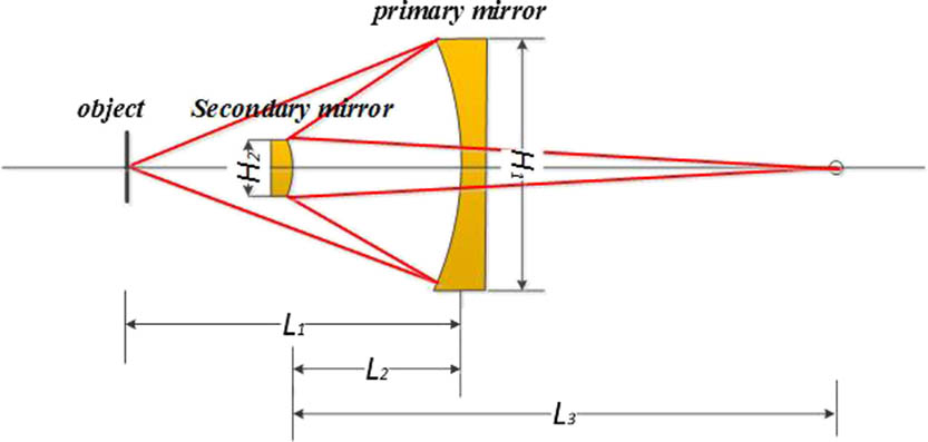
The optical structure of a Schwarzschild microscope is shown in Fig. 1:
Figure 1.Optical structure of the Schwarzschild microscope.
is the object distance, is the gap between the primary and secondary mirrors, is the image distance, and , are apertures of the primary and secondary mirrors.
The spherical mirror imaging formulas are and the formulas of eliminating third-order spherical aberrations and comas[26] are where , are the curvature radius of the primary and secondary mirror, respectively, , are the magnification of the microscope and the secondary mirror, and is the obstruction ratio of the secondary mirror to the primary one.
If we want to obtain a 200 nm mesh edge image by the CCD, which can distinguish two pixels in most instances, so one pixel of the CCD in the object must be up to 100 nm, the magnification can be calculated by
Meanwhile, the object resolution of the Schwarzschild system also needs to be within 200 nm, so the image spatial frequency can be calculated by
This requires the image spatial frequency to be better than 39 lp/mm at modulation transfer function (MTF), which is the response threshold of the CCD.
The optical diffraction-limited resolution is decided by the NA, which is calculated by
The greater the NA, the better the resolution, so we set NA at 0.2. From Eqs. (1)–(4) and (7), the parameters of the Schwarzschild objective are calculated in Table 1.
L1 (mm)
L2 (mm)
L3(mm)
H1 (mm)
H2 (mm)
R1 (mm)
R2 (mm)
119.659
60.504
3221.000
47.592
9.824
93.452
32.480
Table 1. Parameters of the Schwarzschild Objective
The image spatial resolution of this system is 78 lp/mm (), which meets the demand of theobject resolution.
Because the CCD imaging area is , the object FOV can be calculated by
Figures 3(a) and 3(b) show object resolutions along with the change of object distance at different FOVs through the Zemax software:
Figure 3.Object resolutions along with the change of object distance at different FOVs: (a) 1 to 1200 nm resolution; (b) zoomed-in view of the 0 to 450 nm resolutions in (a).
The abscissa 0 point in Figs. 3(a) and 3(b) is the best object point to which the primary mirror distance is 119.659 mm. An abscissa negative direction means that the object distance is far away from the Schwarzschild objective, and the positive direction is the opposite. The object distance moves every 0.5 μm; object resolutions will be worse than 200 nm at different FOVs in the Fig. 3(a). So we simulate for further study the object resolutions that are gotten by the object distance moving every 0.1 μm in Fig. 3(b). In order to keep the resolution within 200 nm in a 100 μm FOV in theory, the change of object distance must not exceed 0.5 μm (from to 0.2 μm).
Figure 4 shows object resolutions along with the change of image distance at different FOVs through the Zemax software:
Figure 4.Object resolutions along with the change of image distance at different FOVs.
The abscissa 0 point in Fig. 4 is the best image point to which the secondary mirror distance is 3221.000 mm. An abscissa positive direction means the image distance is far away from the Schwarzschild objective; a negative direction is the opposite. The image distance moves every 2 mm. In order to keep the resolution within 200 nm in a 100 μm FOV in theory, the change of image distance must not exceed 9 mm (from to 3 mm).
There are three errors that influence the imaging quality of the Schwarzschild objective: one is the figure error of the mirrors and the others are mirror-adjustment errors (centering error and position error on the axes). To achieve a high object resolution, the RMS value of the figure error of the mirrors must be small enough. We bought the spherical mirrors from Winlight company[28], which provides mirrors with an RMS value of the figure errors of 1.02 nm in a spatial frequency from 0.0149 to (primary mirror) and 1.37 nm in a spatial frequency from 0.0763 to (secondary mirror), respectively. Then the mirrors are coated with a Mo/Si multilayer in our group[29]. A centering instrument by Trioptics is used to control the centering error of the mirrors in 2 μm, and a high-precision lathe is used to control the position error of the mirrors on the axes in 20 μm. The MTF curves for different errors are shown in Fig. 5.
From Fig. 5, the system object resolution without errors can be calculated by
By the same formula, the object resolution with figure error , with mirror-centering error , and on-axis position error can be calculated using
Considering these errors, the ultimate object resolution of the Schwarzschild objective can be calculated by
This experiment is completed in a vacuum chamber, the 13.5 nm EUV light comes from a Cu cylindrical target that is irradiated by an Nd:YAG laser with 800 mJ of a single laser pulse energy and 10 ns pulse width. The peak reflectivity of the Mo/Si multilayer can achieve 65% at 13.5 nm, so the total transmission of the Schwarzschild objective is about 42%. A Zr filter of 0.4 μm thickness is used for letting 13.5 nm light pass away and eliminating visible light. The best object resolution needs an accurate object distance, which is hard to find indeed. Meanwhile, the image distance is a fixed value in the vacuum chamber. We use a high-precision 1-axis nanopositioning system by Physik Instrumente (PI) (GmbH & Co. KG) to maintain the precision of the object distance. The moving range of the nanopositioning system with a 0.01 μm precision is 100 μm. Then we put a freestanding gold grid on it as an object. The experimental schematic is shown in Fig. 6.
Figure 6.Schematic of the source and the Schwarzschild imaging system.
In order to guarantee enough EUV light intensity on the CCD, we use the least number of reflectors possible in the light path and the grid is put as close as possible to Cu target. The real precision of nanopositioning with vibration error is 0.5 μm, so we find the best object distance through the change of nanopositioning every 0.5 μm; the image is shown in Fig. 7.
Figure 7.Best imaging figure and the intensity profile.
In Fig. 7, two points of pixel size of the mesh edge were selected. The value of each pixel size is 100 nm. On the top left corner (), if we consider the width at which the density changes from 25% to 75% as an indication of resolution, the pixel is about 2, therefore the best object resolution is about 200 nm. On the bottom right corner (), the object resolution is about 360 nm.
Because the object distance has a great influence on the imaging quality, we move the object distance every 0.5 μm from the best point on the nanopositioning to get some images; the compared results between the simulation and experiment are shown in Fig. 8.
Figure 8.Comparison of the results between the simulation and experiment.
The experimental results are all integer multiples of the CCD pixel, so it is slightly worse than the simulative results with the abovementioned three errors of mirrors. At the abscissa 0 point, the simulative resolution is obviously better than the experimental resolution that is limited by the CCD pixel size.
In order to increase the precision of the results, the best object points were imaged ten times in each experiment.
From Fig. 9, a single optimal object resolution is about 200 nm. Taken an average of ten times, the best object resolution is about 230 nm.
In conclusion, a Schwarzschild microscope is designed to image a mesh edge at a 13.5 nm wavelength. The NA and magnification of the microscope are 0.2 and 130, respectively. A CCD is used as a detector with an imaging area of and pixel size of . To obtain a theoretical resolution of 200 nm within the FOV of 100 μm, the changes of object distance and imaging distance must not separately exceed 0.5 μm and 9 mm. About 200 nm of a single best object resolution is obtained from the experiment in the laboratory, and the average object resolution of 230 nm can be reached, meanwhile, we obtain about 360 nm of object resolution at 80 μm FOV. As a result, we can use a Schwarzschild microscope with a high magnification and high resolution to read micro-object structures of the hundred nanometer level by CCD quickly and intuitively. Meanwhile, the resolution can be further enhanced by using a smaller pixel size detector with a higher magnification or changing the Schwarzschild objective to an aspherical system to enlarge the FOV.
References
[1] S. Chen, S. Ma, Z. Wang. Chin. Opt. Lett., 14, 123401(2016).