• Photonics Research
  • Vol. 11, Issue 4, 526 (2023)
Ali Maleki1, Avinash Singh1, Ahmed Jaber1, Wei Cui1..., Yongbao Xin2, Brian T. Sullivan2, Robert W. Boyd1,3,4 and Jean-Michel Ménard1,*|Show fewer author(s)
Author Affiliations
  • 1Department of Physics, University of Ottawa, Ottawa, Ontario K1N 6N5, Canada
  • 2Iridian Spectral Technologies Ltd, Ottawa, Ontario K1G 6R8, Canada
  • 3School of Electrical Engineering and Computer Science, University of Ottawa, Ottawa, Ontario K1N 6N5, Canada
  • 4Institute of Optics and Department of Physics and Astronomy, University of Rochester, Rochester, New York 14627, USA
  • show less
    DOI: 10.1364/PRJ.472109 Cite this Article Set citation alerts
    Ali Maleki, Avinash Singh, Ahmed Jaber, Wei Cui, Yongbao Xin, Brian T. Sullivan, Robert W. Boyd, Jean-Michel Ménard, "Metamaterial-based octave-wide terahertz bandpass filters," Photonics Res. 11, 526 (2023) Copy Citation Text show less
    (a) General schematic of the bilayer-metamaterial (BLMM) bandpass filter. Two plasmonic metasurfaces are placed adjacent to each other separated by a dielectric coupling layer of thickness d. Each metasurface consists of an array of a metallic square-loop hole structure deposited on Zeonor, a THz transparent substrate. The lattice pitch (P), length of the outer square-loop hole (L), and length of the inner square-loop hole (w) of the array are labeled with black arrows. (b) 3D atomic force microscope (AFM) image and (c) optical microscope image of the device S2, and (d) corresponding depth profile indicating a metal depth of ∼220 nm. (e) THz power transmittance of the commercial double-sided adhesive tapes from Nitto and 3TC used in the fabrication of the BLMM and 2BLMM devices. In this experiment, the double-sided tapes are laminated on a Zeonor substrate and the spectral transmission measured through that substrate is also displayed (black line).
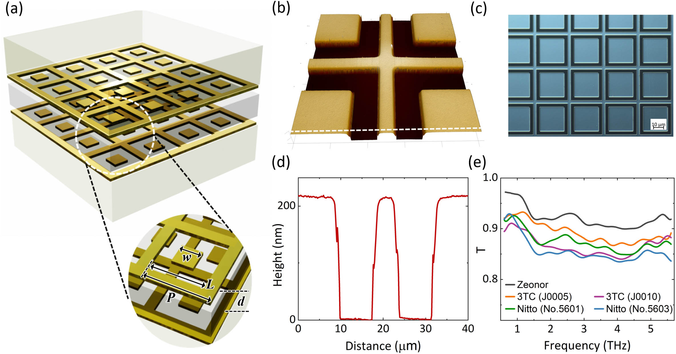
    Fig. 1. (a) General schematic of the bilayer-metamaterial (BLMM) bandpass filter. Two plasmonic metasurfaces are placed adjacent to each other separated by a dielectric coupling layer of thickness d. Each metasurface consists of an array of a metallic square-loop hole structure deposited on Zeonor, a THz transparent substrate. The lattice pitch (P), length of the outer square-loop hole (L), and length of the inner square-loop hole (w) of the array are labeled with black arrows. (b) 3D atomic force microscope (AFM) image and (c) optical microscope image of the device S2, and (d) corresponding depth profile indicating a metal depth of 220  nm. (e) THz power transmittance of the commercial double-sided adhesive tapes from Nitto and 3TC used in the fabrication of the BLMM and 2BLMM devices. In this experiment, the double-sided tapes are laminated on a Zeonor substrate and the spectral transmission measured through that substrate is also displayed (black line).
    THz measured (circles) and simulated (solid lines) transmittance spectrum of the BLMM-based broad bandpass filters in (a) linear scale and (b) semi-logarithmic scale. Experiments are performed with a time-domain THz spectroscopy system and are in good agreement with FDTD simulation results. (c) Measured maximum transmission (Tmax) of the structures over center frequency in semilogarithmic scale, in which error bars present the corresponding octave-spanning FWHM linewidth. (d) Calculated fractional bandwidth (in percentage) of all BLMM devices over frequency for the experiment results.
    Fig. 2. THz measured (circles) and simulated (solid lines) transmittance spectrum of the BLMM-based broad bandpass filters in (a) linear scale and (b) semi-logarithmic scale. Experiments are performed with a time-domain THz spectroscopy system and are in good agreement with FDTD simulation results. (c) Measured maximum transmission (Tmax) of the structures over center frequency in semilogarithmic scale, in which error bars present the corresponding octave-spanning FWHM linewidth. (d) Calculated fractional bandwidth (in percentage) of all BLMM devices over frequency for the experiment results.
    Normalized electric field amplitude distribution of the BLMM structure S5. The arrows indicate surface current distribution within one period of the array. (a) Top view distribution in x−y plane at the surface of the bottom layer plasmonic structure (z=0.2 μm) at the frequency of 2.9 THz. (b) and (c) Side view of the electrical field distribution and direction in the x−z plane, corresponding to a 2D cross section taken at y=−8 μm at a frequency of 2.9 THz and 3.6 THz, respectively. The gray 3D schematics in (b) and (c) illustrate the simulated unit cell of the stacked metasurfaces. The incident THz wave propagates in the z direction and is polarized along the x direction.
    Fig. 3. Normalized electric field amplitude distribution of the BLMM structure S5. The arrows indicate surface current distribution within one period of the array. (a) Top view distribution in xy plane at the surface of the bottom layer plasmonic structure (z=0.2  μm) at the frequency of 2.9 THz. (b) and (c) Side view of the electrical field distribution and direction in the xz plane, corresponding to a 2D cross section taken at y=8  μm at a frequency of 2.9 THz and 3.6 THz, respectively. The gray 3D schematics in (b) and (c) illustrate the simulated unit cell of the stacked metasurfaces. The incident THz wave propagates in the z direction and is polarized along the x direction.
    (a) Schematic of the 2BLMM devices fabricated from two BLMM structures bound together with double-sided tape (separated by a length D). Comparison of the measured THz transmission of the BLMM (blue curve) and 2BLMM (orange curve) devices for (b) S2 and (c) S4. Dotted lines show the averaged attenuation floor.
    Fig. 4. (a) Schematic of the 2BLMM devices fabricated from two BLMM structures bound together with double-sided tape (separated by a length D). Comparison of the measured THz transmission of the BLMM (blue curve) and 2BLMM (orange curve) devices for (b) S2 and (c) S4. Dotted lines show the averaged attenuation floor.
    Measured THz transmittance spectrum of two batches (lines and circles) of the BLMM-based broad bandpass filters in (a) linear scale and (b) semi-logarithmic scale. There is a good repeatability between the pairs of S2, S3, S4, and S6 devices fabricated in two batches and characterized on two different days.
    Fig. 5. Measured THz transmittance spectrum of two batches (lines and circles) of the BLMM-based broad bandpass filters in (a) linear scale and (b) semi-logarithmic scale. There is a good repeatability between the pairs of S2, S3, S4, and S6 devices fabricated in two batches and characterized on two different days.
    DeviceP (μm)L (μm)w (μm)d (μm)Tapef0 (THz)Δf (THz)
    S186806033No. 56030.840.58
    S270664833No. 56031.000.77
    S352483623J0010 and No. 56011.460.86
    S429231710No. 56013.101.57
    S528241610No. 56013.172.02
    S632281533No. 56033.443.20
    Table 1. Geometrical Parameters of the Broad Bandpass Devicea
    StudyStructureBandpass FWHM (THz)Roll-off (dB/octave)FBW (%)Attenuation (dB)
    Current designsSquare-loop hole0.5–3.250–10050–9330–50
    Ref. [19]Skewed circular slot0.8530.251.77
    Ref. [19]Meandered slots0.4544.66010
    Ref. [19]Jerusalem cross slots0.4558.382.210
    Ref. [21]Square slot (fishnet)0.43715
    Ref. [24]Cross slot0.69747630
    Ref. [16]Custom-shape slot0.47656730
    Table 2. Performance Comparison of the Filters Presented in This Work to Similar Structures Based on Layered Metasurfaces Reported in the Literature
    Ali Maleki, Avinash Singh, Ahmed Jaber, Wei Cui, Yongbao Xin, Brian T. Sullivan, Robert W. Boyd, Jean-Michel Ménard, "Metamaterial-based octave-wide terahertz bandpass filters," Photonics Res. 11, 526 (2023)
    Download Citation