
Ting Zhi, Tao Tao, Xiaoyan Liu, Junjun Xue, Jin Wang, Zhikuo Tao, Yi Li, Zili Xie, Bin Liu. Low-threshold lasing in a plasmonic laser using nanoplate InGaN/GaN[J]. Journal of Semiconductors, 2021, 42(12): 122803
- Journal of Semiconductors
- Vol. 42, Issue 12, 122803 (2021)
Abstract
1. Introduction
Due to small physic scale and low power dissipation, miniaturized lasers are important for high resolution displays[
In the work, plasmonic nanolaser based on nanoplate InGaN/GaN was designed via increasing interface area and symmetry at room temperature, which consisted of gain material (nanoplate InGaN/GaN), low refractive index medium (thin SiO2 film) and noble metal film (Silver layer). The threshold is calculated to be ~6.36 kW/cm2, where the FWHM drops from 27 to 4 nm. Moreover, the fast decay time at 502 nm (sharp peak of stimulated lasing) is estimated to be 0.42 ns, indicating a much faster radiative channel. The design plasmonic laser using nano-plate of gain material relatively decreases the edge-scattering ratio, enhances overlap of SPs and excitons, and further holds strong confinement of electromagnetic wave in the low refractive index material.
2. Experimental section
2.1. Growth of gain material
The gain material (GaN/InGaN) was grown on sapphire (0002) substrate by metal-organic chemical vapour deposition (MOCVD). N2 and H2 act as carrier gases for the growth of InGaN and GaN epitaxial layers. After growth, the gain material consisted of a 2 μm undoped GaN buffer layer, a 2 μm silicon-doped n-type GaN layer, 15 periods (InxGa1–xN: 3.5 nm/GaN: 12 nm) of multiple quantum wells (MQWs), a 25 nm Al0.25Ga0.75N layer as an electron-blocking layer, and a 500 nm-thick Mg-doped p-type GaN layer. The In composition (x) was set to be 0.35 in the MQWs region for green emission.
2.2. Fabrication of nano-plate
First of all, the gain material was cleaned with acetone, methanol and then deionized water. In order to form nano-plate, custom-made nano-mask and following inductively coupled plasma (ICP) etching process are necessary. Thus, a thick SiO2 layer (~300 nm) was deposited on the gain material sample as the hard mask, where plasma-enhanced chemical vapour deposition (PECVD) was applied at 300 °C. Subsequently, a thin PMMA layer was spin-coated and patterned by electron beam lithography (EBL). The width and length of nano-sized pattern were set as 0.2 and 1 μm, respectively. The pattern on PMMA layer were reversed in order to acquiring nano-sized metal mask after lift-off process. Therefore, 20 nm-thick nickel were deposited by physical vapor deposition (PVD 75, Kurt J. Lesker) on PMMA layer and lifted-off by warm 1-methyl-2-pyrrolidinone. One more reactive-ion etching (RIE) process was carried out to transform nickel pattern into SiO2 layer as a second reinforced mask. Finally, the gain material with nickel and SiO2 patterned masks was etched using ICP system, where the height of gain material can be controlled to be 3 μm. A set of chemical treatments were carried out: the hot (80 °C) potassium hydroxide for 8 min and following the nitric acid for 2 min, which effectively minimized the surface roughness and defects caused by the ICP etching.
2.3. Preparation of substrate
A undoped silicon substrate was prepared by cleaning with acetone, methanol and then deionized water. A 300 nm SiO2 layer was deposited by PECVD as an insulation material. It has been widely reported that smooth metal surface could dramatically reduce losses, including ohmic and scattering losses[
2.4. Characterization of SPASER
The surface morphology of the samples was measured using a JEOL JSM 7000F field emission scanning electron microscopy (SEM). The photoluminescence (PL) spectra were collected by confocal microscopy equipped with a 40× UV objective lens (Mitutoyo, numerical aperture = 0.5). The lasing beam was focused on a 5 μm-diameter spot coving the whole nano samples at an incident angle of 90°. For fluorescence lifetime measurements, a commercial time-resolved photoluminescence (TRPL) system with time-correlated single photon counting (TCSPC) module was applied, where a 375 nm picosecond laser with pulse width of ~40 ps was used as the excitation source. The parameters for TRPL system were calibrated before for the measurements of all samples.
3. Results and discussion
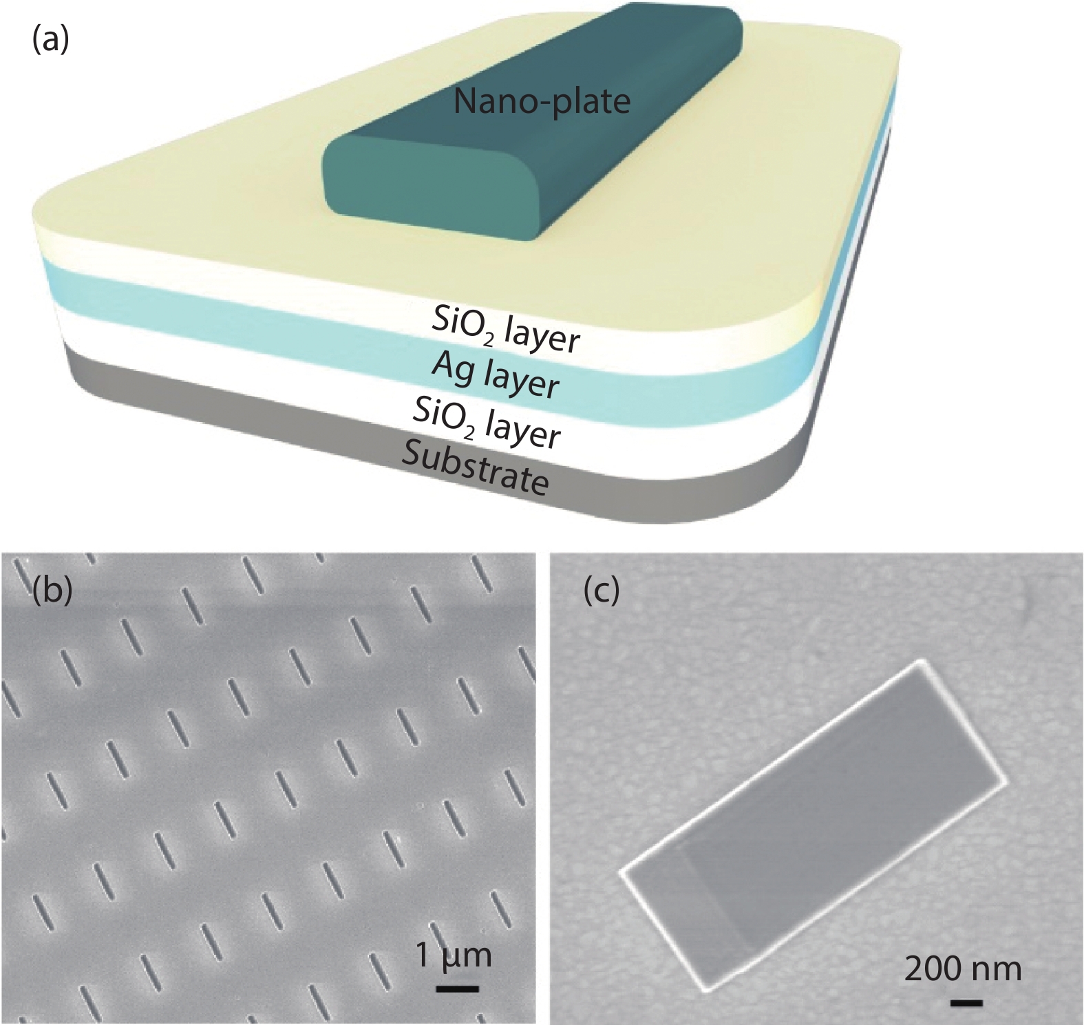
Fig. 1(a) shows the schematic structure of the SPASER, which consists of GaN/InGaN nano-plate, ultra-thin SiO2 layer, the Ag film, SiO2 insulation layer and Si substrate. After EBL and ICP etching process, The SEM image in Fig. 1(b) displays the nano-plate arrays of gain material with a configuration of 200 nm in width, 1 μm in length and 3 μm in height. After mechanical cut and transfer nano-plate onto the prepared Si substrate, nano-plate based SPASER samples are prepared as illustrated by the SEM image in Fig. 1(c). It has been widely reported that rough surface and defects on the sidewall of gain material will cause scattering loss and optical leakage, which limits the corresponding gain from SPs[
![]()
Figure 1.(Color online) (a) Schematic of the nano-plate based SPASER sample, where a thin nano-plate atop silver layer separated by a 10 nm SiO2 gap. (b) SEM image of nano-plate arrays. (c) SEM image of SPASER with single nano-plate (200 nm in width, 1
The photoluminescence (PL) spectra of single nano-plate without Ag film were measured by increasing the optical pumping power density using a micro-PL system excited by a continuous 405-nm laser. A typical spontaneous emission of InGaN/GaN nano-plate can be seen in Fig. 2(a). As the optical pumping power density increasing from 1.27 to 19.11 kW/cm2, the emission peak shifts to 501 nm, indicating a typical spontaneous emission behavior due to the band filling effect and carrier screen in InGaN/GaN gain material[
![]()
Figure 2.(Color online) (a) The PL spectra of nano-plate without Ag film under different optical pumping power density. (b) Corresponding L–L curve of the PL peak intensity and the FWHM in the log–log scale as a function of optical pumping power density. (c) PL emission of SPASER with increasing the same optical pumping power density. (d) Corresponding L–L curve and FWHM of the dominant lasing peak at 502 nm as a function of the excited power density.
On the other hand, sharp peaks appear at 502 nm for SPASER samples under a very low pumping power density, as shown in Fig. 2(c). A small peak shift from 510 to 502 nm with respect to the increasing pumping power reveal a reduced frequency pulling effect due to the strong coupling between SPs and excitons. In Fig. 2(d), an obvious nonlinear “S” shape can be seen, where the lasing threshold can be roughly estimated to be 6.36 kW/cm2. Near the lasing threshold, the FWHM drops from 27 to 4 nm, further confirming the transition from spontaneous emission to stimulated emission. And the quality factor[
The simulated electric field of nano-plate based SPASER samples with/without Ag film was obtained via finite-difference time-domain calculations (FDTD Solutions from Lumerical Solutions). In the simulation, a dipole source was used as a light source with a wide spectral range from 200 to 600 nm. The Ag parameter was adopted from the dielectric function of Palik, and the refraction index of the SiO2 was measured to be 1.46 by an ellipsometer. As illustrated by the simulated cross-sectional electric field distribution in Fig. 3(a), the electromagnetic field can be highly confined within the low-permittivity SiO2 layer with an ultra-small volume in SPASER structure. In another word, the electromagnetic field was confined into an extremely thin waveguide, which is as much as 10 times smaller than the diffraction-limited spot. It should be mentioned that the nano-plate SPASER designed in this work, compared to the cylinder structure in our previous reports[
![]()
Figure 3.(Color online) (a) Simulated electric field distribution of plasmonic laser at 502 nm. (b) Simulated electric field distribution of the Nano-plate gain material without Ag film at 520 nm.
To further understand the mechanism of exciton recombination in SPASER, μ-TRPL of the nano-plate and SPASER were preformed at room temperature and shown in Fig. 4. A standard 2-exponential component model was calculated to study the carrier dynamics for emission. The TRPL traces can be described by[
![]()
Figure 4.(Color online) TRPL spectra of SPASER at the peak of 502 nm (red line) and InGaN/GaN nano-plate at the peak of 520 nm (black line).
where A1 and
4. Conclusion
In summary, new plasmonic laser was designed and demonstrated at visible wavelength based on the nano-plate SPASER structure, consisting of gain material (InGaN/GaN nano-plate), low refractive index medium (thin SiO2 film) and noble metal film (silver layer). The designed nano-plate gain material holds strong confinement of electromagnetic wave in the low refractive index material, where larger interface area enhances the overlap of SPs and excitons and decrease the edge-scattering ratio. As a result, the room temperature lasing threshold is reduced to be ~6.36 kW/cm2, where the FWHM drops from 27 to 4 nm. The present work paves the way for light communication, data storage applications, biological application, especially for optoelectronic devices integrated into a system on a chip.
Acknowledgements
The authors acknowledge financial support from the National Natural Science Foundation of China (62004104, 61974062, 61921005), the Nature Science Foundation of Jiangsu Province (BK20180747 and BE2015111), the Solid State Lighting and Energy-saving Electronics Collaborative Innovation Center, and Research Funds from NJU-Yangzhou Institute of Opto-electronics.
References
[1] X M Goh, Y H Zheng, S J Tan et al. Three-dimensional plasmonic stereoscopic prints in full colour. Nat Commun, 5, 1(2014).
[2] E Murphy. Enabling optical communication. Nature Photon, 4, 287(2010).
[3] Y C Chen, Q S Chen, X D Fan. Lasing in blood. Optica, 3, 809(2016).
[4] M Tchernycheva, A Messanvi, A de Luna Bugallo et al. Integrated photonic platform based on InGaN/GaN nanowire emitters and detectors. Nano Lett, 14, 3515(2014).
[5] M T Hill, Y S Oei, B Smalbrugge et al. Lasing in metallic-coated nanocavities. Nat Photonics, 1, 589(2007).
[6] S W Chang, T R Lin, S L Chuang. Theory of plasmonic fabry-perot nanolasers. Opt Express, 18, 15039(2010).
[7] S L McCall, A F J Levi, R E Slusher et al. Whispering-gallery mode microdisk lasers. Appl Phys Lett, 60, 289(1992).
[8] R M Ma, X L Wei, L Dai et al. Light coupling and modulation in coupled nanowire ring-Fabry-Pérot cavity. Nano Lett, 9, 2697(2009).
[9] D J Bergman, M I Stockman. Surface plasmon amplification by stimulated emission of radiation: Quantum generation of coherent surface plasmons in nanosystems. Phys Rev Lett, 90, 027402(2003).
[10] R F Oulton, V J Sorger, T Zentgraf et al. Plasmon lasers at deep subwavelength scale. Nature, 461, 629(2009).
[11] R M Ma, R F Oulton, V J Sorger et al. Room-temperature sub-diffraction-limited plasmon laser by total internal reflection. Nat Mater, 10, 110(2011).
[12] Y J Lu, C Y Wang, J Kim et al. All-color plasmonic nanolasers with ultralow thresholds: Autotuning mechanism for single-mode lasing. Nano Lett, 14, 4381(2014).
[13] A González-Tudela, P A Huidobro, L Martín-Moreno et al. Theory of strong coupling between quantum emitters and propagating surface plasmons. Phys Rev Lett, 110, 126801(2013).
[14] S W Eaton, A Fu, A B Wong et al. Semiconductor nanowire lasers. Nat Rev Mater, 1, 1(2016).
[15] S L Liu, B W Sheng, X Q Wang et al. Molecular beam epitaxy of single-crystalline aluminum film for low threshold ultraviolet plasmonic nanolasers. Appl Phys Lett, 112, 231904(2018).
[16] Y G Ma, X Guo, X Q Wu et al. Semiconductor nanowire lasers. Adv Opt Photon, 5, 216(2013).
[17] Q Zhang, G Li, X Liu et al. A room temperature low-threshold ultraviolet plasmonic nanolaser. Nat Commun, 5, 4953(2014).
[18] P F Tian, J J D McKendry, E D Gu et al. Fabrication, characterization and applications of flexible vertical InGaN micro-light emitting diode arrays. Opt Express, 24, 699(2016).
[19] T Tao, T Zhi, B Liu et al. Manipulable and hybridized, ultralow-threshold lasing in a plasmonic laser using elliptical InGaN/GaN nanorods. Adv Funct Mater, 27, 1703198(2017).
[20] T Tao, T Zhi, B Liu et al. Electron-beam-driven III-nitride plasmonic nanolasers in the deep-UV and visible region. Small, 16, 1906205(2020).
[21] B Liu, R Smith, M Athanasiou et al. Temporally and spatially resolved photoluminescence investigation of (
[22] B Liu, R Zhang, Z L Xie et al. Nonpolar m-plane thin film GaN and InGaN/GaN light-emitting diodes on LiAlO2(100) substrates. Appl Phys Lett, 91, 253506(2007).

Set citation alerts for the article
Please enter your email address
© Copyright 2018-2021 | Chinese Laser Press. All Rights Reserved 沪ICP备15018463号-20