• Chinese Physics B
  • Vol. 29, Issue 8, (2020)
Lanting Ji1、2, Wei Chen1, Yang Gao1, Yan Xu1, Chi Wu2, Xibin Wang1, Yunji Yi1, Baohua Li1, Xiaoqiang Sun1、†, and Daming Zhang1
Author Affiliations
  • 1State Key Laboratory of Integrated Optoelectronics, College of Electronic Science & Engineering, Jilin University, Changchun 3002, China
  • 2Institute of Marine Science and Technology, Shandong University, Qingdao 50100, China
  • show less
    DOI: 10.1088/1674-1056/ab943b Cite this Article
    Lanting Ji, Wei Chen, Yang Gao, Yan Xu, Chi Wu, Xibin Wang, Yunji Yi, Baohua Li, Xiaoqiang Sun, Daming Zhang. Low-power electro–optic phase modulator based on multilayer graphene/silicon nitride waveguide[J]. Chinese Physics B, 2020, 29(8): Copy Citation Text show less
    (a) Three-dimensional (3D) and (b) cross-sectional view of the graphene-based Si3N4 waveguide electro–optic modulator.
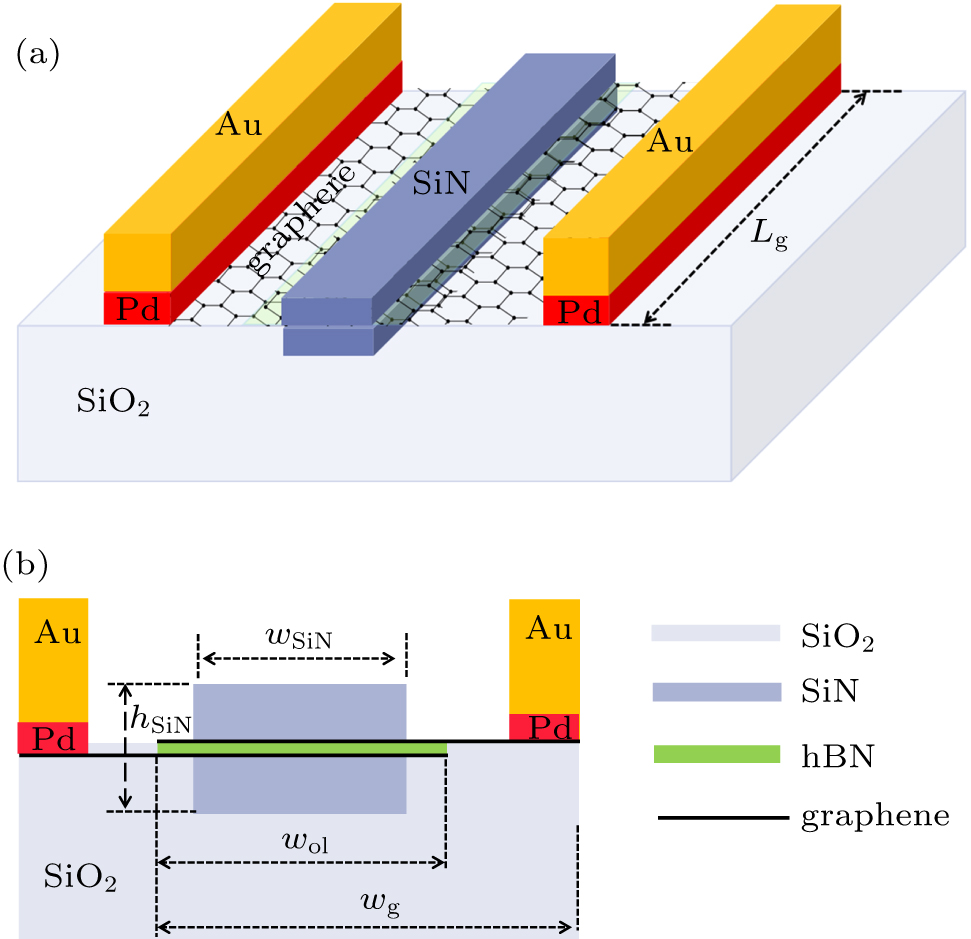
    Fig. 1. (a) Three-dimensional (3D) and (b) cross-sectional view of the graphene-based Si3N4 waveguide electro–optic modulator.
    In-plane permittivity changes with Fermi level μc of graphene at 1550 nm.
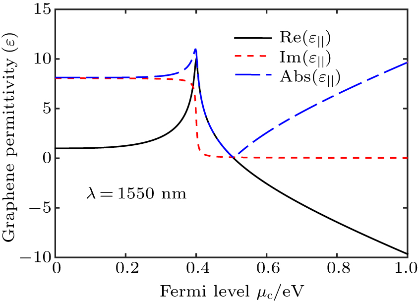
    Fig. 2. In-plane permittivity changes with Fermi level μc of graphene at 1550 nm.
    Im(Neff) of SiN waveguide as a function of hSiN and wSiN when μc is 0 eV (λ = 1550 nm).
    Fig. 3. Im(Neff) of SiN waveguide as a function of hSiN and wSiN when μc is 0 eV (λ = 1550 nm).
    Cross-section of (a) two-layer, (c) four-layer, and (e) six-layer GSNW configurations. Panels (b), (d), and (f) show field distributions of panels (a), (c), and (e), respectively.
    Fig. 4. Cross-section of (a) two-layer, (c) four-layer, and (e) six-layer GSNW configurations. Panels (b), (d), and (f) show field distributions of panels (a), (c), and (e), respectively.
    (a) Real and (b) imaginary parts of Neff as a function of Fermi level for different graphene layers.
    Fig. 5. (a) Real and (b) imaginary parts of Neff as a function of Fermi level for different graphene layers.
    Illustration of (a) quasi-linear variation of the optical phase, and (b) optical MPA versus Fermi levels for different numbers of graphene layer.
    Fig. 6. Illustration of (a) quasi-linear variation of the optical phase, and (b) optical MPA versus Fermi levels for different numbers of graphene layer.
    Optical transmission of the MZI modulator changes with applied gate voltages for the 80-μm-long graphene with different layers.
    Fig. 7. Optical transmission of the MZI modulator changes with applied gate voltages for the 80-μm-long graphene with different layers.
    Illustration of (a) quasi-linear variation of the optical phase, and (b) insertion loss versus Fermi levels for different graphene modulation lengths.
    Fig. 8. Illustration of (a) quasi-linear variation of the optical phase, and (b) insertion loss versus Fermi levels for different graphene modulation lengths.
    Normalized transmission of the MZI modulator changes with applied gate voltage for the two-layer graphene at different modulating lengths.
    Fig. 9. Normalized transmission of the MZI modulator changes with applied gate voltage for the two-layer graphene at different modulating lengths.
    Equivalent electrical circuits of (a) two-, (b) four-, and (c) six-layer graphene modulators.
    Fig. 10. Equivalent electrical circuits of (a) two-, (b) four-, and (c) six-layer graphene modulators.
    StructureMZI
    Layer number246
    Lg/μm801602408016024080160240
    Ctotal/pF0.3220.6320.9420.6321.2521.8720.9421.8722.802
    Rtotal10.55.253.505.252.631.753.501.751.17
    ΔU/V3.601.020.491.070.340.200.480.190.14
    Power/(pJ/bit)1.0430.1640.0570.1810.0360.0190.0540.0170.014
    f3 dB/GHz47.148.048.348.048.548.648.348.648.6
    IL/dB0.220.440.660.430.861.290.641.281.92
    Table 1. Modulating performance of different GSNW modulators.
    DescriptionLength/μmf3 dB/GHzPower/(pJ/bit)Bias/VInsertion loss/dB
    Graphene on Si WG[17]75.6119.50.45211.37
    Graphene-Si on slot WG[24]100500NA1.30.97
    2-layer graphene in SOI[35]500300.387.80.6
    1-layer graphene in SOI[35]850190.666.52.805
    Graphene on ultrathin Si WG[36]96.6314.20.0973.871.55
    This work (2-layer GSNW)8047.11.0431.080.22
    This work (4-layer GSNW)8048.00.1811.080.43
    This work (6-layer GSNW)8048.30.0541.080.64
    Table 2. Performance comparison between graphene-based phase modulators.
    Lanting Ji, Wei Chen, Yang Gao, Yan Xu, Chi Wu, Xibin Wang, Yunji Yi, Baohua Li, Xiaoqiang Sun, Daming Zhang. Low-power electro–optic phase modulator based on multilayer graphene/silicon nitride waveguide[J]. Chinese Physics B, 2020, 29(8):
    Download Citation