• Chinese Optics Letters
  • Vol. 20, Issue 2, 023601 (2022)
Jingjing Hong1、2, Xingping Zhou1、2, Rui Zhuang1、2, Wei Peng1、2, Jiawei Liu1、2, Aiping Liu1、2、*, and Qin Wang1、2
Author Affiliations
  • 1Institute of Quantum Information and Technology, Nanjing University of Posts and Telecommunications, Nanjing 210003, China
  • 2Key Laboratory of Broadband Wireless Communication and Sensor Network Technology, Ministry of Education, Nanjing University of Posts and Telecommunications, Nanjing 210003, China
  • show less
    DOI: 10.3788/COL202220.023601 Cite this Article Set citation alerts
    Jingjing Hong, Xingping Zhou, Rui Zhuang, Wei Peng, Jiawei Liu, Aiping Liu, Qin Wang. Nanoparticle trapping by counter-surface plasmon polariton lens[J]. Chinese Optics Letters, 2022, 20(2): 023601 Copy Citation Text show less

    Abstract

    A counter-surface plasmon polariton lens (CSPPL) is proposed to perform stable nanoparticle trapping by providing up to 120kbT optical potential depth. The optical potential depth is related to the incident angle and phase difference of the light incident on two gratings of CSPPL. The depth of optical potential can be manipulated with negligible displacement by the incident angle less than 20°. Both the depth and the center position of the optical potential well can be manipulated by the incident phase difference. The study of stable and manipulatable optical potential on the CSPPL promotes the integration of optical tweezers.

    1. Introduction

    Since Ashkin first proposed optical tweezers (OTs) in 1986[1], this device has been widely used in many fields, including biological particle trapping[25], molecular manipulation[6,7], Raman spectroscopy[810], and so on[1116]. Compared to other conventional mechanical tweezers, OTs can capture and manipulate the entire particle in a non-direct contact and damage-free manner, which is suitable for trapping vulnerable particles, especially in biological experiments[17,18].

    However, due to the limited optical gradient force and large volume, the traditional OTs are incapable of trapping particles stably on integrated chips[17,19]. With the development of near-field optics, the application of evanescent waves in OTs provides a more effective particle capture method benefitting from the enhanced light field[20,21]. A surface plasmon polariton (SPP) is one of the surface waves propagating along the metal-dielectric interface, shorter in terms of wavelength than that of the incident light wave, which results in a stronger local electric field intensity and higher spatial precision[2225]. So, SPPs have potential applications in on-chip nanoparticle trapping.

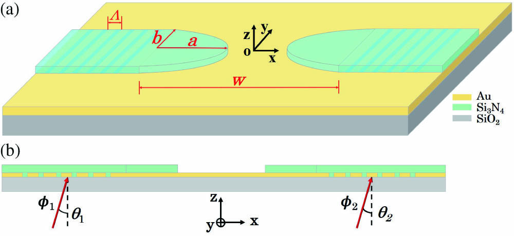
    In this Letter, we propose a counter-SPPs lens (CSPPL), composed of two SPPs lenses on the SiO2 substrate, to trap and manipulate nanoparticles. Counter-propagating SPPs are focused by the CSPPL to produce interference patterns, which can provide a strong optical field to trap nanoparticles. The influences of incident angle and initial phase difference on the interference fringes are also studied, which shows that the pattern of interference fringes can be monitored freely on the CSPPL.

    2. Principle of Theory

    Figure 1(a) illustrates the three-dimensional diagram of the designed CSPPL, where there are two opposite positioned semicircular columns of silicon nitride with semi-major radius a and semi-minor radius b on the Au-SiO2 substrate. The center distance of two semicircular columns is w. Two gratings with a period of Λ are fully etched on the Au film under the waveguides, which are connected to the semicircular columns, respectively. The coordinate origin point is set at the center of the CSPPL.

    Schematic illustration of the proposed CSPPL: (a) 3D view; (b) cross section of y = 0.

    Figure 1.Schematic illustration of the proposed CSPPL: (a) 3D view; (b) cross section of y = 0.

    As depicted in Fig. 1(b), two Gaussian beams are incident on the gratings with incident angles of θi and initial phases of ϕi (i=1, 2) from the SiO2 substrate to excite SPPs [22]. The polarization direction of the incident beams is perpendicular to the gratings to obtain a high excitation efficiency of SPPs.

    The excited SPPs propagating along the waveguide will be manipulated by the semicircular column of the CSPPL as a focusing lens to change the propagation path of SPPs. Two focusing SPPs traveling from opposite directions interfere with each other to form the stronger and weaker interference fringes at the center of the CSPPL. The standing waves generated by the interference provide strong and concentrated field intensity for nanoparticles trapping.

    When the radius of the nanoparticle is much smaller than the wavelength of light, it can be taken as a Rayleigh particle in the interaction with the light field. The gradient force of the light field acting on the nanoparticle can be expressed as[21]F(r)=αε0|E(r)|2/4,where α=Vεm(εεm)/ε2εm is the polarizability of the particles with a volume of V. ε0, ε, and εm are the dielectric constants of vacuum, particle, and background medium, respectively. E is the electric field. r=(x,y,z) is the location of the particle. Since the axial radiation scattering forces from two counter directions of propagation are cancelled, it is reasonable to neglect the scattering force[21,26]. So, the optical trapping potential at any point can be calculated by integrating the gradient force along an appropriate path, which can be given asU(r0)=r0F(r)·dr.

    In other words, the optical trapping potential is the energy needed to remove the trapped nanoparticle from the trapping point r0 to the infinity. On the basis of Ashkin’s stability criterion, the depth of optical potential well U is required to be more than 10kbT for stable trapping. In the following analysis, we use this standard to verify whether the designed structure can satisfy the stable particles trapping.

    3. Results

    The field distribution of SPPs on the CSPPL is given by the method of finite-difference time-domain (FDTD). The parameters used in the simulation are as follows: the gratings period Λ is 360 nm; the semicircular column waveguides are fabricated in the 200 nm depth Au film with a=b=2.5μm and w=9μm. The relative permittivity of Au is 23.0211+1.43641i, corresponding to an incident wavelength of 785 nm[27]. The refractive indices of Si3N4 and SiO2 are 1.99 and 1.45, respectively[28,29]. The whole structure is immersed in water with refractive index nw=1.33 [30]. The electric field distributions in three planes are displayed in Fig. 2 with 1 W incident light on each grating, which is the same in the following. Figure 2(a) is the intensity distribution on the xy plane 100 nm above the surface of the Au film, which shows a standing wave with multiple nodes. The intensity distributions of the electric field in the cross sections of x=0 and y=0 are shown in Figs. 2(b) and 2(c), respectively. The intensity of the evanescent wave decays exponentially when it is far away from the surface of the Au film.

    Intensity distributions of electric field in (a) z = 0.1 µm plane, (b) x = 0 plane, and (c) y = 0 plane.

    Figure 2.Intensity distributions of electric field in (a) z = 0.1 µm plane, (b) x = 0 plane, and (c) y = 0 plane.

    The interference field formed on the CSPPL provides an optical potential well for trapping particles. The optical forces for the Au nanoparticle with a radius of 35 nm are calculated as shown in Fig. 3. The optical forces along the x direction, y direction, and z direction are given, respectively, in Figs. 3(a), 3(b), and 3(c), where different colors of curves correspond to different semi-major radii a with the same b=2.5μm. As shown in Figs. 3(a) and 3(b), the optical trapping forces Fx and Fy are zero at the center point (x=0, y=0). When the Au nanoparticle is away from the center point, the optical forces Fx and Fy increase and are directed to the center point, which make the nanoparticle move to the center point. In the z direction, the optical force Fz is directed to the Au surface and increases as the Au nanoparticle is far away from the Au surface, as shown in Fig. 3(c), which makes the nanoparticle close to the surface. Considering the size of the nanoparticle and the roughness of the substrate, the optical force along the z direction is calculated from 50 nm above the surface. The effective depth of the optical potential well with 1 W incident light on each grating is given in Table 1. The trap of the nanoparticle is mainly considered on the xy plane, so the trapping potential in the z direction is not given. The optical potentials are all above 10kbT, which meet the Ashkin’s stability criterion for nanoparticle trapping.

    The optical force is different for the CSPPL with different radii, since the focused SPP is due to the refraction on the arc surface of the semicircular column. For the proposed CSPPL, the focus points of two SPPs are closest to the center of the CSPPL with a=2.9μm, and the strongest optical trapping force is formed on the center for all three directions. So, the CSPPL with a=2.9μm and b=2.5μm is considered in the following analysis.

    Radius a (μm)2.32.52.72.93.1
    Ux (kbT)63.0699.1484.09123.1789.88
    Uy (kbT)64.96104.0688.11129.9294.49

    Table 1. Depth of Optical Potential Wells with Different Semi-Major Radii

    Optical force along the (a) x direction, (b) y direction, and (c) z direction for different semi-major radii a, respectively.

    Figure 3.Optical force along the (a) x direction, (b) y direction, and (c) z direction for different semi-major radii a, respectively.

    The electric field distribution on the CSPPL is formed by the interference of the SPPs from two gratings, so it is related to the incident phase on the gratings. Figures 4(a)4(e) show the electric field distributions along the x direction with the incident phase difference Δϕ=0, 90°, 180°, 270°, and 360°, respectively. It is found that the electric field in the center changes from bright to dark gradually as Δϕ increases from 0° to 180° and changes back to bright as Δϕ increases from 180° to 360°. At the same time, the position of the interference fringes moves to right along the x direction as the incident phase difference increases with a period of 360°.

    Intensity distributions of the electric field in the x–y plane with (a)–(e) different incident phase differences Δϕ and (f)–(j) different incident angles θ2.

    Figure 4.Intensity distributions of the electric field in the x–y plane with (a)–(e) different incident phase differences Δϕ and (f)–(j) different incident angles θ2.

    The electric field distribution is also related to the incident angle, as shown in Figs. 4(f)4(j). With fixed θ1=0°, the interference fringes of the electric field move to right at first and then move to left as θ2 increases. When two beams are incident perpendicularly to the grating with θ1=θ2=0°, the brightest antinode is on the center. When θ2 increases from 0° to 34°, the brightest antinode moves to right, leaving a dark node on the center of the CSPPL. The brightest antinode moves back to the center as the θ2 increases to 43°, as shown in Fig. 4(j).

    The incident phase can be changed freely, so the optical potential formed by the electric field is manipulatable. The displacement of the center antinodes in the x direction is shown in Fig. 5(a), where the displacement increases as the incident phase difference Δϕ increases. It is obvious that the optical potential depth decreases as the phase difference increases in both directions in Fig. 5(b). So, both the position and the depth of the optical potential can be manipulated by the incident phase difference with a period of 360°.

    Effect of the incident phase difference Δϕ and the incident angle θ2 on the potential well. (a) Displacement of the center antinode along the x direction as a function of the incident phase difference. (b) Optical potential as a function of the incident phase difference. (c) Displacement of the center antinode along the x direction as a function of the incident angle. (d) Optical potential as a function of the incident angle.

    Figure 5.Effect of the incident phase difference Δϕ and the incident angle θ2 on the potential well. (a) Displacement of the center antinode along the x direction as a function of the incident phase difference. (b) Optical potential as a function of the incident phase difference. (c) Displacement of the center antinode along the x direction as a function of the incident angle. (d) Optical potential as a function of the incident angle.

    Figure 5(c) gives the displacement of the brightest antinode in the x direction as a function of the incident angle θ2. When the incident angle changes from 0° to 20°, the displacement of the brightest antinode in the x direction is negligible. When the incident angle further increases to 34°, the center antinode has a maximum displacement of 0.08 µm. Figure 5(d) gives the relation of the optical potential of the brightest antinode and the incident angle. The optical potential depth increases first to obtain the deepest at θ2=8° and then decreases. This is because the best phase matching is obtained to excite the SPPs with θ2=8°. The optical potential of the brightest antinode has a depth of about 190kbT with negligible displacement when θ2=8° and θ1=0°, which is beneficial to the nanoparticle trapping. So, the optical potential depth can be manipulated with the incident angle with negligible displacement of the trapping center.

    4. Conclusion

    In conclusion, the structure of the CSPPL is proposed to provide manipulatable optical potential for trapping nanoparticles in integrated optics. The designed CSPPL performs a stable capture of the Au nanoparticle with a radius of 35 nm. The incident phase difference can manipulate both the optical potential depth and the optical trapping position at the same time with a period of 360°, while the incident angle can manipulate the optical potential depth without the displacement of trapping center. A manipulatable optical potential will promote the development of optical trapping in integrated optics.

    References

    [1] A. Ashkin, J. M. Dziedzic, J. E. Bjorkholm, S. Chu. Observation of a single-beam gradient force optical trap for dielectric particles. Opt. Lett., 11, 288(1986).

    [2] A. Ashkin, J. M. Dziedzic, T. Yamane. Optical trapping and manipulation of single cells using infrared laser beams. Nature, 330, 769(1987).

    [3] M. Zhou, H. Yang, J. Di, E. Zhao. Manipulation on human red blood cells with femtosecond optical tweezers. Chin. Opt. Lett., 6, 919(2008).

    [4] B. S. Ahluwalia, P. McCourt, T. Huser, O. G. Hellesø. Optical trapping and propulsion of red blood cells on waveguide surfaces. Opt. Express, 18, 21053(2010).

    [5] O. G. Hellesø, P. Løvhaugen, A. Z. Subramanian, J. S. Wilkinson, B. S. Ahluwalia. Surface transport and stable trapping of particles and cells by an optical waveguide loop. Lab. Chip., 12, 3436(2012).

    [6] Y. Pang, R. Gordon. Optical trapping of a single protein. Nano Lett., 12, 402(2012).

    [7] F. Properzi, M. Logozzi, S. Fais. Exosomes: the future of biomarkers in medicine. Biomark. Med., 7, 769(2013).

    [8] F. Svedberg, Z. Li, H. Xu, M. Käll. Creating hot nanoparticle pairs for surface-enhanced Raman spectroscopy through optical manipulation. Nano Lett., 6, 2639(2006).

    [9] J. Shen, J. Wang, C. Zhang, C. Min, H. Fang, L. Du, S. Zhu, X. C. Yuan. Dynamic plasmonic tweezers enabled single-particle-film-system gap-mode surface-enhanced Raman scattering. Appl. Phys. Lett., 103, 191119(2013).

    [10] A. Yang, L. Du, X. Dou, F. Meng, C. Zhang, C. Min, J. Lin, X. Yuan. Sensitive gap-enhanced Raman spectroscopy with a perfect radially polarized beam. Plasmonics, 13, 991(2018).

    [11] J. Yu, X. Tong, C. Li, Y. Huang, A. Ye. Using optical tweezers to investigate the specific single-interaction between apoA-I molecule and ABCA1 on living cells. Chin. Opt. Lett., 11, 091701(2013).

    [12] G. Rui, Q. Zhan. Trapping of resonant metallic nanoparticles with engineered vectorial optical field. Nanophotonics, 3, 351(2014).

    [13] X. Peng, C. Chen, B. Chen, Y. Peng, M. Zhou, X. Yang, D. Deng. Optically trapping Rayleigh particles by using focused partially coherent multi-rotating elliptical Gaussian beams. Chin. Opt. Lett., 14, 011405(2016).

    [14] P. Polimeno, A. Magazzù, M. A. Iatì, F. Patti, R. Saija, C. D. Esposti Boschi, M. G. Donato, P. G. Gucciardi, P. H. Jones, G. Volpe, O. M. Maragò. Optical tweezers and their applications. J. Quantum Spectrosc. Radiat. Transfer, 218, 131(2018).

    [15] G. Rui, Y. Li, S. Zhou, Y. Wang, B. Gu, Y. Cui, Q. Zhan. Optically induced rotation of Rayleigh particles by arbitrary photonic spin. Photon. Res., 7, 69(2019).

    [16] A. Huang, D. Chen, H. Li, D. Tang, B. Yu, J. Li, J. Qu. Three-dimensional tracking of multiple particles in large depth of field using dual-objective bifocal plane imaging. Chin. Opt. Lett., 18, 071701(2020).

    [17] A. Ashkin, J. M. Dziedzic. Optical trapping and manipulation of viruses and bacteria. Science, 235, 1517(1987).

    [18] A. Ashkin. History of optical trapping and manipulation of small-neutral particle, atoms, and molecules. IEEE J. Sel. Top. Quantum Electron., 6, 841(2000).

    [19] F. M. Fazal, S. M. Block. Optical tweezers study life under tension. Nat. Photon., 5, 318(2011).

    [20] D. G. Kotsifaki, S. N. Chormaic. Plasmonic optical tweezers based on nanostructures: fundamentals, advances and prospects. Nanophotonics, 8, 1227(2019).

    [21] C. Bai, J. Chen, Y. Zhang, S. Kanwal, D. Zhang, Q. Zhan. Shift of the surface plasmon polariton interference pattern in symmetrical arc slit structures and its application to Rayleigh metallic particle trapping. Opt. Express, 28, 21210(2020).

    [22] T. W. Ebbesen, H. J. Lezec, H. F. Ghaemi, T. Thio, P. A. Wolff. Extraordinary optical transmission through sub-wavelength hole arrays. Nature, 391, 667(1998).

    [23] X. Ren, A. Liu, C. Zou, L. Wang, Y. Cai, F. Sun, G. Guo, G. Guo. Interference of surface plasmon polaritons from a “point” source. Appl. Phys. Lett., 98, 201113(2011).

    [24] L. Zhang, L. Wang, Y. Wu, R. Tai. Plasmonic Luneburg lens and plasmonic nano-coupler. Chin. Opt. Lett., 18, 092401(2020).

    [25] K. Mujeeb, M. Faryad, A. Lakhtakia, J. V. Urbina. Surface-plasmonic sensor using a columnar thin film in the grating-coupled configuration [Invited]. Chin. Opt. Lett., 19, 083601(2021).

    [26] X. Xu, D. J. Thomson, J. Yan. Optimisation and scaling effect of dual-waveguide optical trapping in the SOI platform. Opt. Express, 28, 33285(2020).

    [27] P. B. Johnson, R. W. Christy. Optical constants of the noble metals. Phys. Rev. B, 6, 4370(1972).

    [28] H. R. Philipp. Optical properties of silicon nitride. J. Electrochem. Soc., 120, 295(1973).

    [29] E. D. Palik. Handbook of Optical Constants of Solids, 3(1998).

    [30] G. M. Hale, M. R. Querry. Optical constants of water in the 200-nm to 200-µm wavelength region. Appl. Opt., 12, 555(1973).

    Jingjing Hong, Xingping Zhou, Rui Zhuang, Wei Peng, Jiawei Liu, Aiping Liu, Qin Wang. Nanoparticle trapping by counter-surface plasmon polariton lens[J]. Chinese Optics Letters, 2022, 20(2): 023601
    Download Citation