Abstract
We demonstrate a silicon-based microwave photonic filter (MPF) with flattop passband and adjustable bandwidth. The proposed MPF is realized by using a 10th-order microring resonator (MRR) and a photodetector, both of which are integrated on a photonic chip. The full width at half-maximum (FWHM) bandwidth of the optical filter achieved at the drop port of the 10th-order MRR is 21.6 GHz. The ripple of the passband is less than 0.3 dB, while the rejection ratio is 32 dB. By adjusting the deviation of the optical carrier wavelength from the center wavelength of the optical bandpass filter, the bandwidth of the MPF can be greatly changed. In the experiment, the FWHM bandwidth of the proposed MPF is tuned from 5.3 to 19.5 GHz, and the rejection ratio is higher than 30 dB.1. INTRODUCTION
As the demand for capacity in radio frequency (RF) telecommunication keeps increasing, traditional microwave research based on the electrical technique has become increasingly challenging over time. With inherent advantages such as low loss, large bandwidth, immunity to electromagnetic interference (EMI), excellent tunability, and reconfigurability, microwave photonics is a promising candidate to confront this challenge [1–3]. As one of the key branches of signal processing in microwave photonics, the microwave photonic filter (MPF) has been intensively studied ever since its emergence, and many MPFs with various functions have been demonstrated [4–11]. MPFs with single passband or stopband can effectively extract or suppress the desired signals. When such MPFs have adjustable bandwidths, more flexibility is achieved in the system [12–16]. Stimulated Brillouin scattering (SBS) is an effective approach to implementing MPF with a high rejection ratio. By changing the bandwidth of the optical pump of the SBS, the bandwidth of the achieved MPF can be adjustable [12,13]. The tuning range of the bandwidth depends on the bandwidth of the optical pump, but a larger bandwidth of optical pump means more power consumption of the system. Based on an optical comb source and a dispersive medium, a reconfigurable and tunable flattop MPF is demonstrated and the full width at half-maximum (FWHM) of this filter can be adjusted from 1.5 to 2.5 GHz [14]. In 2012, Chen et al. proposed an MPF with adjustable bandwidth based on phase modulation and cascaded Bragg gratings [15]. By adjusting the optical carrier wavelength, an MPF with bandwidth adjustable from 3.5 to 5.5 GHz is acquired after the photodetector (PD). In 2015, Li et al. proposed a reconfigurable MPF based on a polarization modulator (PolM) and an optical bandpass filter [16]. When the phase modulation on two orthogonal polarization states is tuned and then combined, both the shape and bandwidth of the achieved MPF can be changed. The FWHM bandwidth can be adjusted from 5 to 11 GHz. However, MPFs based on discrete optoelectronic devices are bulky and expensive. In order to reduce the volume and cost and improve reliability, monolithic integration is a very promising technique. Therefore, photonic chip-based MPF with adjustable bandwidth was also proposed and demonstrated [17,18]. Benefiting from the narrow bandwidth of SBS gain, the on-chip SBS-based MPFs exhibit high factor, and the achieved largest FWHM bandwidth is 440 MHz [18]. In order to implement SBS, an optical pump is necessary in the system, so the schemes are more complex, and further integration of the systems will also face more challenges.
In this paper, we demonstrate a silicon-on-insulator (SOI)-based MPF with flattop and single passband. A 10th-order microring resonator (MRR) is integrated with a PD on a photonic chip. By controlling the resonant wavelength of each MRR, the 10th-order MRR could achieve a flattop optical filter at its drop port. The FWHM bandwidth of the optical filter is 21.6 GHz. The ripple of the passband is less than 0.3 dB, while the rejection ratio is 32 dB. When a phase-modulated signal is asymmetrically attenuated by the optical filter, the phase-modulated signal is converted to an intensity signal. After PD, a single-bandpass MPF can be achieved, and its rejection ratio is more than 30 dB. By tuning the wavelength of the optical carrier, the bandwidth of the MPF can be adjusted. Benefiting from the large passband of the optical filter, the FWHM bandwidth of the proposed MPF can be widely adjusted from 5.3 to 19.5 GHz.
2. PRINCIPLE
The principle of the proposed MPF is shown in Fig. 1. The optical carrier with angular frequency of is phase-modulated by an RF signal with an angular frequency of . For the small-signal modulation condition, only the st order sidebands are considered, and the optical field after modulation can be expressed as where denotes the amplitude of the input light, denotes the th order of the first kind Bessel functions, and denotes the modulation index of the RF signal, respectively. Then the optical signal is sent into the optical filter shown in Fig. 1, and the optical field after the optical filter can be expressed as where , , and denote the attenuation coefficients of the optical carrier, the st sideband, and the st sideband, respectively. The filtered optical signal is then injected into the PD, and the photocurrent can be described as where is the responsivity of the PD. Since , Eq. (3) can be simplified as When the frequency of the optical carrier is tuned aligned with the center of the optical filter, shown in Fig. 1(a), the two sidebands will be symmetrically filtered so . According to Eq. (4), the two beating signals will be cancelled by each other. When the frequency of the carrier is detuned away from the center of the optical filter, shown in Fig. 1(b), the attenuation of the two sidebands is asymmetrical. The frequency difference between the optical carrier and the right edge of the optical filter passband is marked as . When , , and there will be a zero output of the PD. Within the optical filter passband and when , we can get . From Eq. (4), it can be concluded that frequencies in the asymmetrical region marked by blue dashed lines in Fig. 1(b) will lead to a microwave bandpass filter response after the PD. By tuning within the passband of the optical filter, the asymmetrical region is also changed, and the bandwidth of the formed MPF is changed correspondingly.
Sign up for Photonics Research TOC. Get the latest issue of Photonics Research delivered right to you!Sign up now
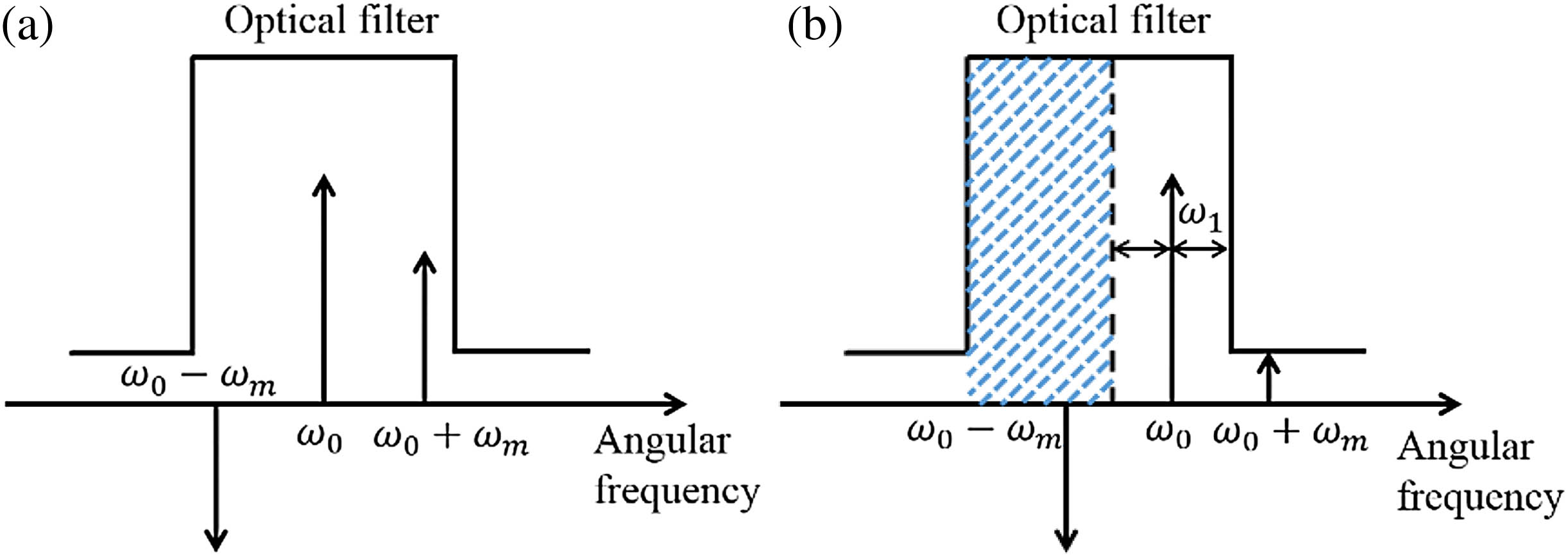
Figure 1.Optical spectra of the phase-modulated signal and the flattop optical filter when the frequency of the optical carrier is tuned (a) aligned with the center of the optical filter and (b) away from the center of the optical filter.
3. DEVICE DESIGN, SIMULATION, AND FABRICATION
In order to achieve the flattop optical filter, an SOI-based photonic chip is designed; its structure is shown in Fig. 2. It mainly consists of a 10th-order MRR and an integrated PD. The optical wave is coupled into the 10 cascaded MRRs via grating coupler (GC1), and the output at the drop port is sent into the integrated PD. The high-order MRR is designed to have a flattop passband at the drop port. In order to overcome the misalignment caused by fabrication deviation [19–21], the microheater is deposited on each MRR and used to adjust the resonant wavelength of the MRR. By adjusting the voltages applied to the heaters, the resonant wavelengths of the MRRs can be aligned, and an optical bandpass filter is realized. GC2 and GC3 are designed to measure and monitor the adjustment of the transmission spectrum of the 10th-order MRR. When measuring the transmission spectrum of the 10th-order MRR, the broadband light is coupled into the chip via GC2, and the transmitted light is coupled out of the chip via GC3. By comparing the input and output spectra, the transmission spectrum of the 10th-order MRR can be achieved, and the adjustment of the resonant wavelengths can be implemented.

Figure 2.Structure of the photonic chip.
In order to reduce the optical loss of the waveguide, a rib waveguide is applied in the device. The full silicon layer thickness is 220 nm. The rib is etched to a depth of 130 nm, and the width of the rib is 500 nm. According to these parameters, the simulated result of the group refractive index is 3.897. The diameters of the 10 MRRs are all designed to be 81.6 μm. The relationship between the diameter and the free spectral range (FSR) of the MRR can be expressed as where refers to the speed of light in vacuum, refers to the group refractive index, and refers to the length of the MRR. According to Eq. (5), the FSR of the MRR is 150 GHz. To implement a flattop filter at the drop port, the 11 self-coupling coefficients of the two strip waveguides and 10 MRRs are symmetrically designed as 0.741, 0.954, 0.9747, 0.9747, 0.9747, 0.98, 0.9747, 0.9747, 0.9747, 0.954, and 0.741 [22].
The simulated result of the output at the drop port of the 10th-order MRR is shown in Fig. 3(a). The FWHM bandwidth is 18.1 GHz, and the power ripple of the flattop is less than 0.3 dB. Based on the simulated result of the 10th-order MRR and the theoretical analysis of the proposed MPF, the simulated results of the MPF can be achieved. As can be seen in Fig. 3(b), the achieved MPF is a flattop bandpass filter, and the flatness of the passband can keep almost invariant while the FWHM bandwidth is tuned from 5.0 to 18.7 GHz. In the simulation, the rejection ratio of the MPF exceeds 50 dB.
Figure 3.Simulated results of (a) output at the drop port of the 10th-order MRR and (b) proposed MPF with adjustable bandwidths.
The optical micrograph of the fabricated device is shown in Fig. 4. The 10 MRRs are fabricated according to the designed parameters, and each ring has an individual heater on its top. Each heater is connected with an individual metal electrode, while the other end of each heater is connected with the grounded electrode. The waveguide coupled Ge PD is used to transform the light into electrical signal. The Ge is grown on top of the shallow etched silicon area for light absorption. The width, length, and height of the Ge region are designed to be 5 μm, 10 μm, and 0.5 μm, respectively.
Figure 4.Optical micrograph of the fabricated device.
It can be noted that there is a phase modulator (PM) placed between the 10th-order MRR and the PD, as shown in Fig. 4. The PM is originally designed to be monolithically integrated with the cascaded MRRs and PD. However, serious electromagnetic cross talk between the electrical signals applied to the PM and PD can be observed. Therefore, in the experiment, an external PM is used to replace the silicon-based one.
4. EXPERIMENTAL RESULTS
Because of fabrication deviation, the center wavelengths of the cascaded MRRs are usually not aligned [19–21]. Therefore, microheaters are deposited on each MRR and used to tune the resonant wavelength. The experimental setup of tuning the MRRs is illustrated in Fig. 5. A broadband optical source (BOS, Amonics ALS-18-B-FA) is connected with a polarization beam splitter (PBS) to make the optical source linearly polarized. Then, the linearly polarized light is adjusted to be aligned with the TM mode of fabricated waveguides via the polarization controller (PC). The broadband light is input into the chip via GC2 (Fig. 5) and coupled out of the chip via GC3. The output spectrum is measured by an optical spectrum analyzer (OSA, Ando AQ6319). By controlling the voltages applied to the heaters, the resonant wavelength of each MRR will be changed. To get a flattop bandpass filter at the drop port of the 10th-order MRR, the heaters of the 10 separate MRRs must be controlled precisely. The voltages of the 10 heater electrodes shown in Fig. 4 are set as 10.51, 1.47, 4.34, 4.73, 5.34, 1.96, 1.82, 0.45, 10.55, and 2.00 V from right to left, respectively; the measured optical bandpass filter is shown in Fig. 6. Since the flattop of the 10th-order MRR is superposed by the 10 individual MRRs, the shape of the flattop will be influenced by each of the 10 rings. Moreover, because of the thermal cross talk, the change of bias voltage applied to one microheater also affects adjacent MRRs, which increases the difficulty in adjusting the MRRs. However, during our experiment, once the voltage of each MRR is adjusted to the optimal situation, the state of the 10th-order MRR is fixed, and the stability of the 10th-order MRR can be ensured. So, the bandwidth adjustment of the MPF is realized by tuning the optical carrier instead of tuning the microheaters of the MRRs in the experiment. In order to reduce the thermal cross talk between rings, the thermal isolation trenches can be designed, and the heating efficiency can be improved as well [23,24]. From Fig. 6, it can be observed that a flattop optical bandpass filter is achieved. The rejection ratio of this optical filter is 32 dB, and the FWHM bandwidth is 21.6 GHz, while the ripple of the flattop is less than 0.3 dB. Compared with the simulated result, the FWHM bandwidth of the measured optical filter is a little wider, and the rejection ratio is smaller. As we have mentioned above, the fabrication deviations of the 10 MRRs also cause the deviations of the self-coupling coefficients. In simulation, the 10th-order MRR is in perfect condition, which means the 10 MRRs are identical, and the self-coupling coefficients are exactly the same as designed. During the fabrication of the device, the perfect condition is impossible to be met because of the fabrication deviation. Therefore, the bandwidth of the achieved optical filter differs from the simulated result, and the rejection ratio of the achieved optical filter deteriorates compared with the simulated result.
Figure 5.Experimental setup of tuning the 10th-order MRR. BOS, broadband optical source; PBS, polarization beam splitter; PC, polarization controller; OSA, optical spectrum analyzer.
Figure 6.Optimized optical filter at the drop port.
The scheme of the proposed MPF is illustrated in Fig. 7. A continuous-wave (CW) light emitted from a laser diode (LD, Alnair TLG-200) is launched into the PM (Covega LN66S-FC) after PC1. The PM is driven by the RF signals emitted from the vector network analyzer (VNA, Anritsu, MS4647B). Then, after the polarization is adjusted by PC2, the phase-modulated optical signal is coupled into the 10th-order MRR via GC1. Then the phase-modulated signal is asymmetrically attenuated by the MRR-based optical bandpass filter and converted to intensity signal, which is detected by the integrated PD. The output RF signal is amplified by an electrical amplifier (EA, LNA-300K35G) and then received by the VNA.
Figure 7.Experimental setup of the proposed MPF. LD, laser diode; PC, polarization controller; PM, phase modulator; EA, electronic amplifier; VNA, vector network analyzer.
The measured results of the integrated PD are shown in Fig. 8. The dark current is about 0.50 μA when the reverse biased voltage is 3 V. According to the measured photocurrent, the intrinsic responsivity is calculated to be about 1 A/W at 1550 nm under a reverse-biased voltage of 3 V. The frequency response of the PD is shown in Fig. 8(b); the 3 dB bandwidth under 3 V reverse-biased voltage is about 25 GHz.
Figure 8.(a) Measured dark current of the Ge PD; (b) measured response of the Ge PD.
The optical spectrum of the phase-modulated signal is shown as the green dashed curve in Fig. 9 when the flattop filter is bilaterally symmetrical; the beat signal between the optical carrier and the st order sideband will be completely cancelled by the beat signal between the optical carrier and the st order sideband. When the optical carrier deviates from the center of the optical bandpass filter, the symmetry of the phase-modulated signal is broken, shown as the red dotted curve in Fig. 9. The power of the st order sideband is lower than that of the st order sideband. The two beat signals cannot be cancelled by each other, and a flattop MPF is measured by the VNA; this is shown as a red curve in Fig. 10. The measured rejection ratio of the MPF is around 30 dB, and the FWHM bandwidth is 5.3 GHz.
Figure 9.Optical spectra of the bandpass filter and the phase-modulated signals after the filter.
Figure 10.Measured frequency responses of the proposed MPF with different bandwidths.
When the optical carrier is further detuned away from the center of the optical bandpass filter, the bandwidth of the MPF will be increased. The wavelength of the optical carrier is tuned in a step of 0.01 nm, and the corresponding responses are shown in Fig. 10. During the tuning process, the measured MPF remains flattop passband, while its FWHM bandwidth is increased in a step of around 2.4 GHz. When the st order sideband is suppressed, as shown by the blue dashed-dotted curve in Fig. 9, the measured MPF is shown as the blue curve in Fig. 10. The corresponding rejection ratio is about 30 dB, and the FWHM bandwidth is 19.5 GHz. The passband ripple of the proposed MPF is less than 1.8 dB. Since the transmission edge of the realized optical filter is not as sharp as the ideal rectangle-shaped filter shown in Fig. 1, the effective bandwidth of the realized optical filter, which can be used to implement the MPF, is smaller than the measured FWHM bandwidth. This is because the insertion loss of the MPF will be greatly increased if the optical carrier wavelength is located at the slope of the 10th-order MRR optical filter. So the wavelength of the carrier will not be tuned to the edge of the optical filter. Besides, the resolution of the OSA is 0.01 nm, which leads to a measure error of about 1.25 GHz. As a result, the measured bandwidth of the realized MPF is smaller than that of the 10th-order MRR optical filter. The rejection ratio of the realized optical filter and MPF is about 32 and 30 dB, respectively. The selectivity of the MPF coincides well with that of the optical filter. The selectivity of the realized optical filter and MPF can be improved if the problem of fabrication deviation can be reduced.
5. CONCLUSION
An SOI-based integrated MPF with a flattop passband is proposed and successfully demonstrated. A 10th-order MRR and an integrated PD are monolithically integrated. By adjusting the voltages applied to the heaters, the resonant wavelengths of the 10 MRRs are tuned to realize a flattop optical filter. The conversion from phase modulation to intensity modulation is implemented after asymmetrical suppression by the optical filter when the optical carrier wavelength is detuned from the center of the optical filter. By changing the wavelength of the optical carrier, the FWHM bandwidth of the MPF is adjusted from 5.3 to 19.5 GHz, while the rejection ratio remains at more than 30 dB.
References
[1] J. Yao. Microwave photonics. J. Lightwave Technol., 27, 314-335(2009).
[2] J. Capmany, D. Novak. Microwave photonics combines two worlds. Nat. Photonics, 1, 319-330(2007).
[3] A. J. Seeds. Microwave photonics. IEEE Trans. Microw. Theory Tech., 50, 877-887(2002).
[4] Y. Yu, E. Xu, J. Dong, L. Zhou, X. Li, X. Zhang. Switchable microwave photonic filter between high Q bandpass filter and notch filter with flat passband based on phase modulation. Opt. Express, 18, 25271-25282(2010).
[5] F. Jiang, Y. Yu, H. Tang, L. Xu, X. Zhang. Tunable bandpass microwave photonic filter with ultrahigh stopband attenuation and skirt selectivity. Opt. Express, 24, 18655-18663(2016).
[6] X. Xue, X. Zheng, H. Zhang, B. Zhou. Widely tunable single-bandpass microwave photonic filter employing a non-sliced broadband optical source. Opt. Express, 19, 18423-18429(2011).
[7] H. Tang, Y. Yu, C. Zhang, Z. Wang, L. Xu, X. Zhang. Analysis of performance optimization for a microwave photonic filter based on stimulated Brillouin scattering. J. Lightwave Technol., 35, 4375-4383(2017).
[8] M. Bolea, J. Mora, B. Ortega, J. Capmany. Highly chirped single-bandpass microwave photonic filter with reconfiguration capabilities. Opt. Express, 19, 4566-4576(2011).
[9] L. Xu, X. Kong, Z. Wang, H. Tang, X. Liu, Y. Yu, J. Dong, X. Zhang. A tunable single passband microwave photonic filter of overcoming fiber dispersion induced amplitude fading. IEEE Photon. J., 9, 5502008(2017).
[10] X. Liu, Y. Yu, H. Tang, L. Xu, J. Dong, X. Zhang. Silicon-on-insulator-based microwave photonic filter with narrowband and ultrahigh peak rejection. Opt. Lett., 43, 1359-1362(2018).
[11] Y. Yu, H. Tang, L. Xu, X. Liu, F. Jiang, J. Dong, X. Zhang. Switchable microwave photonic filter between low-pass and high-pass responses. IEEE Photon. J., 8, 5501408(2016).
[12] B. Vidal, M. Piqueras, J. Martí. Tunable and reconfigurable photonic microwave filter based on stimulated Brillouin scattering. Opt. Lett., 32, 23-25(2007).
[13] Y. Stern, K. Zhong, T. Schneider, R. Zhang, Y. Ben-Ezra, M. Tur, A. Zadok. Tunable sharp and highly selective microwave-photonic band-pass filters based on stimulated Brillouin scattering. Photon. Res., 2, B18-B25(2014).
[14] M. Song, C. M. Long, R. Wu, D. Seo, D. E. Leaird, A. M. Weiner. Reconfigurable and tunable flat-top microwave photonic filters utilizing optical frequency combs. IEEE Photon. Technol. Lett., 23, 1618-1620(2011).
[15] T. Chen, X. Yi, L. Li, R. Minasian. Single passband microwave photonic filter with wideband tunability and adjustable bandwidth. Opt. Lett., 37, 4699-4701(2012).
[16] W. Li, C. Yang, L. Wang, Z. Yuan, J. Liu, M. Li, N. Zhu. Microwave photonic bandstop filter with wide tunability and adjustable bandwidth. Opt. Express, 23, 33579-33586(2015).
[17] A. Byrnes, R. Pant, E. Li, D.-Y. Choi, C. G. Poulton, S. Fan, S. Madden, B. Luther-Davies, B. J. Eggleton. Photonic chip based tunable and reconfigurable narrowband microwave photonic filter using stimulated Brillouin scattering. Opt. Express, 20, 18836-18845(2012).
[18] A. Choudhary, I. Aryanfar, S. Shahnia, B. Morrison, K. Vu, S. Madden, B. Luther-Davies, D. Marpaung, B. J. Eggleton. Tailoring of the Brillouin gain for on-chip widely tunable and reconfigurable broadband microwave photonic filters. Opt. Lett., 41, 436-439(2016).
[19] C. Chauveau, P. Labeye, J.-M. Fedeli, S. Blaize, G. Lerondel. Study of the uniformity of 300 mm wafer through ring-resonator analysis. IEEE International Conference on Photonics in Switching (PS), 1-3(2012).
[20] L. Chrostowski, X. Wang, J. Flueckiger, Y. Wu, Y. Wang, S. T. Fard. Impact of fabrication non-uniformity on chip-scale silicon photonic integrated circuits. Optical Fiber Communication Conference, Th2A–37(2014).
[21] W. Bogaerts, P. De Heyn, T. Van Vaerenbergh, K. De Vos, S. K. Selvaraja, T. Claes, P. Dumon, P. Bienstman, D. Van Thourhout, R. Baets. Silicon microring resonators. Laser Photon. Rev., 6, 47-73(2012).
[22] F. Xia, M. Rooks, L. Sekaric, Y. Vlasov. Ultra-compact high order ring resonator filters using submicron silicon photonic wires for on-chip optical interconnects. Opt. Express, 15, 11934-11941(2007).
[23] P. Dong, W. Qian, H. Liang, R. Shafiiha, D. Feng, G. Li, J. E. Cunningham, A. V. Krishnamoorthy, M. Asghari. Thermally tunable silicon racetrack resonators with ultralow tuning power. Opt. Express, 18, 20298-20304(2010).
[24] P. Dong, W. Qian, H. Liang, R. Shafiiha, N.-N. Feng, D. Feng, X. Zheng, A. V. Krishnamoorthy, M. Asghari. Low power and compact reconfigurable multiplexing devices based on silicon microring resonators. Opt. Express, 18, 9852-9858(2010).


