
Yueying Zhan, Jianhua He, Fei Wang, Liqian Wang. Analysis and testing of total ionizing dose effect on several commercial optical transceivers via gamma-ray radiation[J]. Chinese Optics Letters, 2019, 17(5): 052302
- Chinese Optics Letters
- Vol. 17, Issue 5, 052302 (2019)
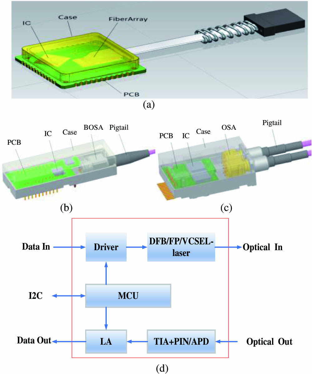
Fig. 1. Internal structure diagram of (a) parallel, (b) single-channel, (c) EPON, and (d) chip relationships of transceivers.
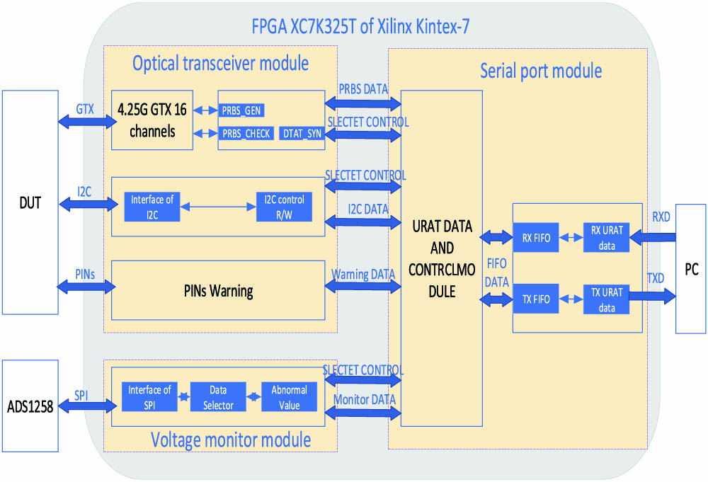
Fig. 2. FPGA block diagram of TID testing.
Fig. 3. Function diagram of the TID testing board.
Fig. 4. Diagram of (a) the TID testing environment, (b) the TID test device, and (c) the upper computer software.
Fig. 5. Current changing of optical modules with the TID.
Fig. 6. Schematic diagram of upper computer software.
Fig. 7. Receiver sensitivity of HTS2361, HTS3261, and HTS8566 at different total doses.
Fig. 8. Eye diagram of (a), (b) HTS3261 at 0 and 50 krad, (c), (d) HTS2361 at 0 and 41 krad, and (e), (f) HTS8566 at 0 and 50 krad.
Fig. 9. Current changing of the first test board with the total dose in the second testing.
Fig. 10. Current changing trend of the second board in the second TID testing.
Fig. 11. Structure of (a) BOSA of the HTS3261, (b) TOSA of HTS8566, and (c) ROSA of HTS8566.
Fig. 12. Relationship between the thickness of the Al shell and the 10-year dose of LEO aircraft.

Set citation alerts for the article
Please enter your email address
© Copyright 2018-2021 | Chinese Laser Press. All Rights Reserved 沪ICP备15018463号-20