
Bowen Zeng, Chenxia Li, Bo Fang, Zhi Hong, Xufeng Jing, "Flexible tuning of multifocal holographic imaging based on electronically controlled metasurfaces," Photonics Res. 12, 61 (2024)
- Photonics Research
- Vol. 12, Issue 1, 61 (2024)
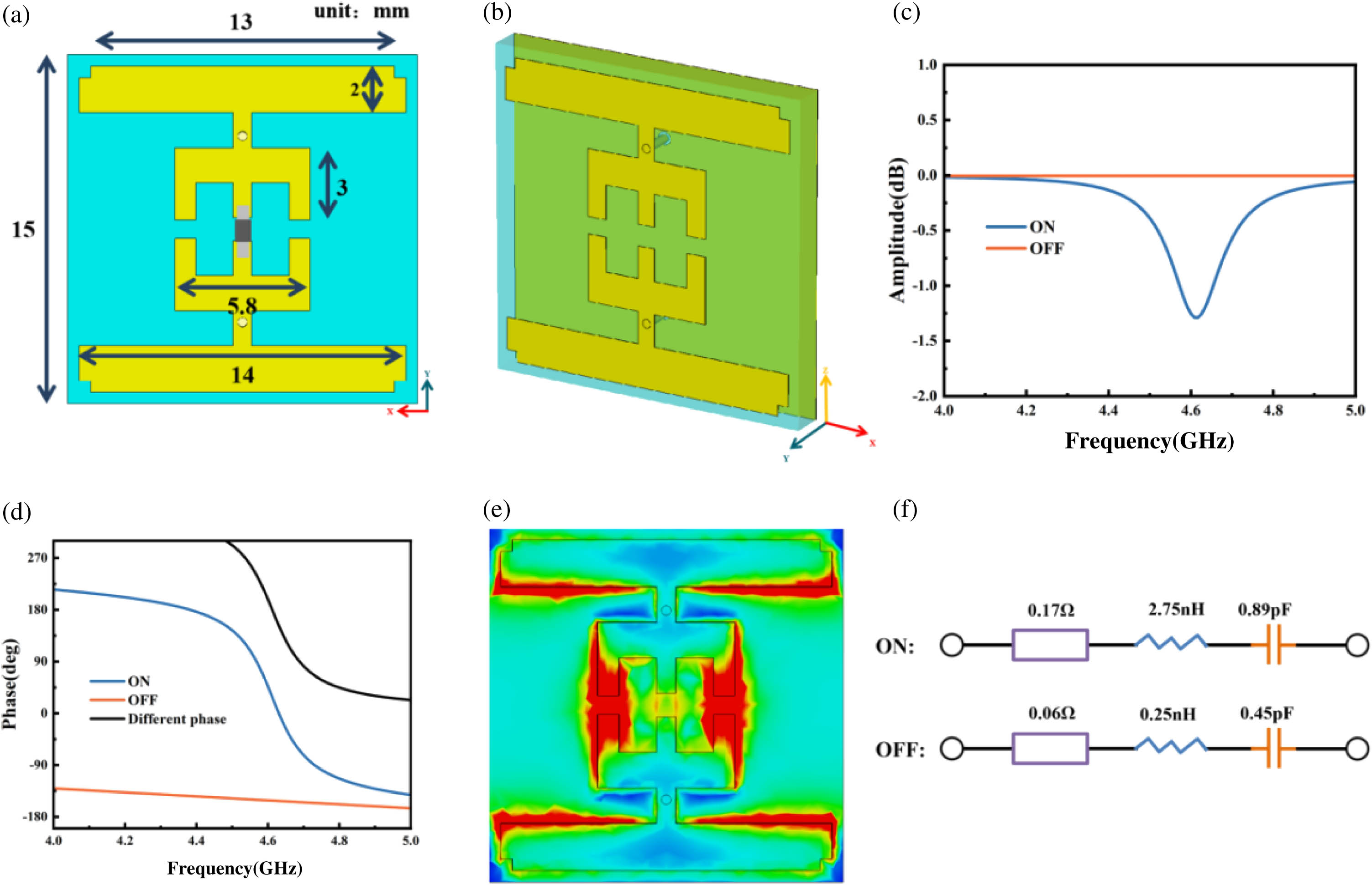
Fig. 1. (a), (b) Schematic of the cell structure, (c) reflection amplitude, (d) reflection phase, (e) surface electric field distribution, and (f) RLC model of the diode in the “ON” and “OFF” states.
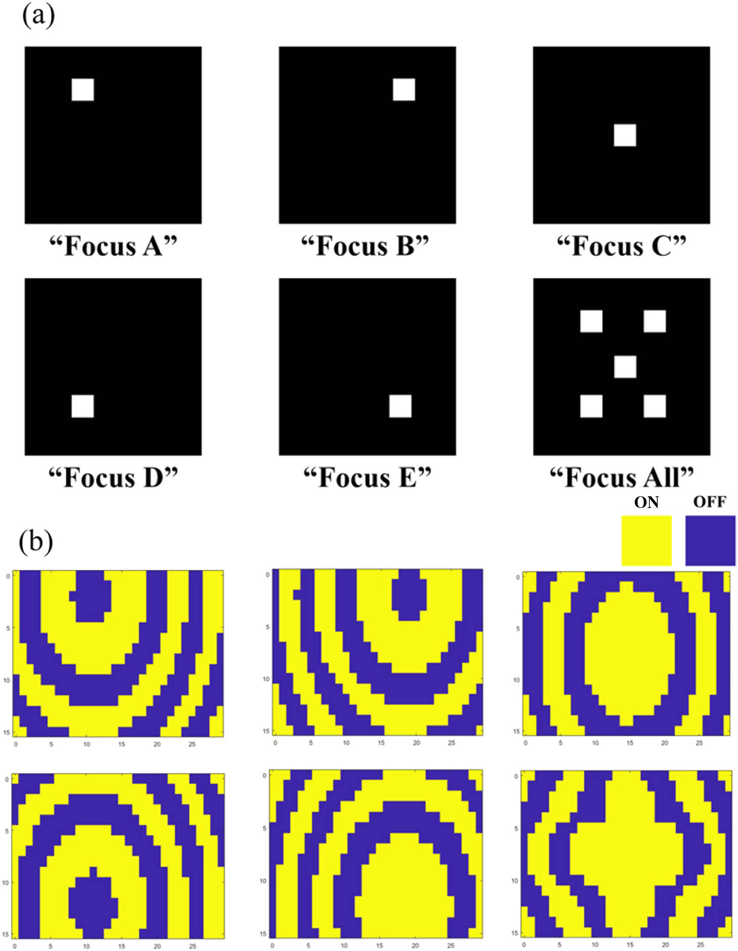
Fig. 2. (a) Grayscale map of each focal point; (b) phase alignment map obtained from GS algorithm calculation.
Fig. 3. Near-field focusing characteristics of the focal spot for each phase arrangement.
Fig. 4. (a) Coding S1 with “focus C” convolution. (b) Coding S2 with “focus C” convolution. (c) Encoding S3 with “focus C” convolution operation.
Fig. 5. (a)–(c) Near-field Z, Y, 3D maps obtained by S1 encoding convolution. (d)–(f) Near-field Z, Y, 3D plots obtained by S2 coded convolution. (g)–(i) Near-field Z, Y, 3D maps obtained by S3 encoded convolution.
Fig. 6. (a) Phase distribution and near-field hologram corresponding to the letter C, (b) phase distribution and near-field hologram corresponding to the letter J, (c) phase distribution and near-field hologram corresponding to the letter L, and (d) phase distribution and near-field hologram corresponding to the letter U.
Fig. 7. (a) Block diagram of the experimental flow, (b) electrical connection diagram, (c) experimental overview diagram, and (d) 3D rendering of a single PCB board on the super surface.
Fig. 8. Diagram of the experimental setup.
Fig. 9. Eight-group multifocal experimental validation plot.


Set citation alerts for the article
Please enter your email address

© Copyright 2018-2021 | Chinese Laser Press. All Rights Reserved 沪ICP备15018463号-20