
Boning Han, Qingsong Shan, Fengjuan Zhang, Jizhong Song, Haibo Zeng. Giant efficiency and color purity enhancement in multicolor inorganic perovskite light-emitting diodes via heating-assisted vacuum deposition[J]. Journal of Semiconductors, 2020, 41(5): 052205
- Journal of Semiconductors
- Vol. 41, Issue 5, 052205 (2020)
Abstract
1. Introduction
Owing to good thermal stability and excellent electrical transport ability, inorganic hybrid perovskite light-emitting diodes (PeLEDs) have drawn significant research attention[
Vapor deposition, a solvent-free deposition procedure, can effectively eliminate solvent damage to the film and improve the film crystallographic quality[
Among perovskite LEDs studies, film crystal quality and morphology management are important for high-quality perovskite film in device construction, which is favorable for carrier radiative recombination in emission layer. For solution process, heating treatment and organic ligand passivation can help film crystallization and optimize film morphology. However, supplementary conditions are difficult to be introduced during film formation in vacuum deposition, so the perovskite films with poor crystallinity and morphology have high defect densities and cannot fully cover the hole transport layer (HTL) or electron transport layer (ETL). Defects and insufficient film coverage result in the reduction of carriers radiative recombination, as well as the formation of shunting paths due to the direct contact between the HTL and ETL[
Herein, heating-assisted vacuum deposition (HAVD) strategy was proposed to prepare perovskite emitting layer for the used in PeLEDs, in which the substrates were heating during the perovskite deposition, and the substrate temperature can be set up by programming. The perovskite crystallization and film surface roughness can be effectively optimized by changing substrate heating temperature, and film with dense and uniform crystal grains and better crystallographic quality was obtained. Outstanding morphology and crystallization of CsPbBr3 films can be finely tuned to reduce defect density and improve carriers radiative recombination for the emitting layer. As a result, CsPbBr3-based green PeLEDs with the maximum luminance of 11 941 cd/cm2 presented a 100-fold improvement in EQE. In addition, the performance of red and blue PeLEDs also can be improved by HAVE method, that the EQE of devices enhanced more than 100 folds. It should be noted that the perovskite film prepared by HAVD have uniform crystal size, and so the full width at half-maximum (FWHM) of electroluminescence (EL) was lower than 20 nm, showing high color purity. This is the first time to reveal the impact of substrate temperature on the performance of the vacuum deposited PeLEDs, and it proves that the HAVD of perovskite film is a common method for LEDs application and potentially develops a road for future exploration of large area and flexibility PeLEDs production with scale-up mode.
2. Experiment and method
2.1. Materials
CsBr, PbBr2, PbI2, PbCl2, poly(ethylenedioxythiophene):polystyrene sulphonate (PEDOT:PSS), Poly(N, N’-bis(4-butylphenyl)-N,N’-bis(phenyl)-benzidine) (poly-TPD), 2′,2′-(1,3,5-benzinetriyl)-tris(1-phenyl-1-H-benzimidazole)) (TPBi), and LiF were purchased from Xi’an Polymer Light Technology Corp. All the chemical materials were directly used without any further purifications.
2.2. Device fabrication
Pre-patterned indium-doped tin oxide (ITO) substrates were sonicated in aceton for 15 min through three times in the beaker to make them clean. Then the ITO substrates were baked in the heating plate at 250 °C for 15 min and followed treated by the UV-Ozone for 15 min. PEDOT:PSS (filtered through a 0.22 μm filter) can be coated on the treated ITO substrates as spin-coating at 3000 rpm for 60 s and baked at 150 °C for 15 min successively. Poly-TPD (6 mg/mL) solution as HTL was subsequently spin-coated at 4000 rpm for 45 s and baked at 150 °C for 15 min. Then, the samples were transferred into the vacuum chamber to deposit the luminous layer and the vacuum degree of the deposition chamber was about 2 × 10⁻⁴ Pa. The PeLEDs have a device structure of ITO/PEDOT:PSS/poly-TPD/perovskite/TPBi/LiF/Al. The perovskite emitting layer was formed by multi-source vacuum thermal evaporation by separated crucibles of CsBr, PbBr2, PbI2, and PbCl2. The ratios of halogen in perovskite films were controlled by the thickness of mixing materials monitored by quartz crystal monitor. The substrates were heated to the set temperature for the deposition of perovskite raw materials, and cooled to room temperature for the deposition of TPBi, LiF and Al.
2.3. Characterization and device measurements
The crystalline structure of perovskite is determined by X-ray diffractometer (Bruker D8 Advance) with Cu Ka radiation source. The atomic force microscopy (AFM) images and roughness analysis are obtained with Bruker Multimode 8 instrument. UV–Vis absorption spectra are tested using a Shimadzu 3600 UV–Vis spectrophotometer (in the 200–800 nm spectral range). The PL spectra of the perovskite films are obtained by using a Varian Cary Eclipse spectrometer. For the time-correlated single photon counting measurements, the samples were excited by 405 nm based picoseconds laser, and the TRPL was analyzed by using F900 software. The device was placed in the integrating sphere in glovebox for testing. The EL spectra and V–J–L characteristics were tested as the voltage as loaded by Keithley 2400, and the light output was detected by a PMA-12 spectrometer at room temperature.
3. Results and discussion
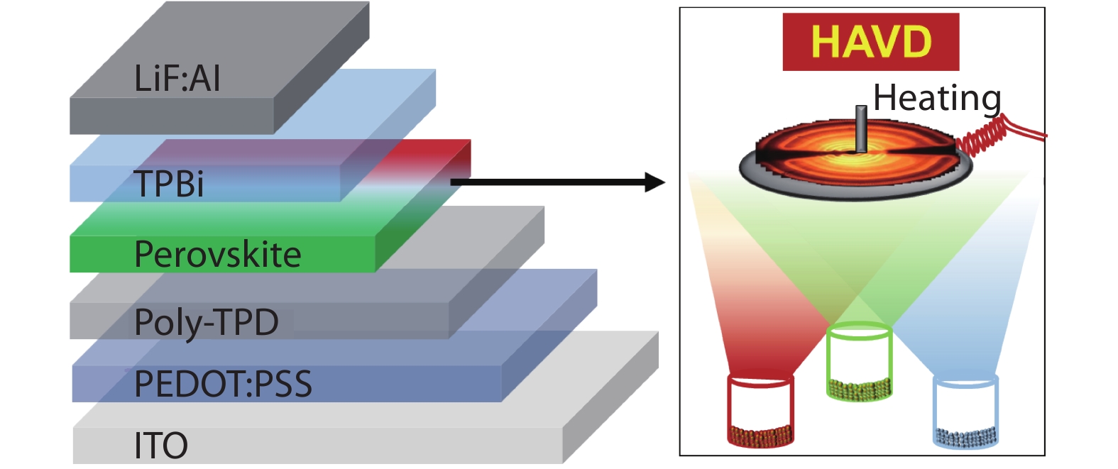
Fig. 1 displays the illustration of device configuration of PeLEDs based on heating-assisted vacuum deposition (HAVD). The hole injection layer (PEDOT:PSS) and hole transfer layer (Poly-TPD)) were successively spin coated on ITO. The substrate was subsequently transferred to vacuum system for the perovskite emitting layer deposition. Unlike conventional deposition. Here, the substrates were heating when perovskite raw materials were deposited. Perovskites were evaporated on ITO/PEDOT:PSS/poly-TPD substrates by controlling the thickness of CsBr and PbBr2/PbI2/PbCl2. Thickness of the individual PbBr2/PbI2/PbCl2 and CsBr layers was calculated according to the molar ratio of 1 : 1.15. Shutters were placed above the material sources to ensure the accuracy of film thickness and material proportion. After finishing the perovskite deposition, the substrates were then cooled to room temperature for electron transfer layer and electrode deposition. The experimental details are provided in the experimental section.
![]()
Figure 1.(Color online) Illustration of multilayer perovskite LED device and the heating-assisted vacuum deposition (HAVD) method to deposit the perovskite film.
Perovskite film with good optical performance is the precondition for radiative recombination in LED device. Fig. 2(a) exhibits the variation of the photoluminescence (PL) of perovskite films deposited on glass substrates as the substrates were kept at room temperature (RT) and heated at 80, 100, and 120 °C. The emission peak of PL spectra was located at 519 nm, and the PL intensity of RT-based film was relatively dim. With increasing substrate heating temperature, the increase in green emission was pretty evident and the PL intensity of 100 °C-based one was improved more than 10 folds compared with the RT-based film. Accordingly, the photoluminescence quantum yield (PLQY) of the perovskite films was enhanced from 1.2% to 35.8% as the substrate temperature was increased to 100 °C, as shown in Fig. 2(b). The inset photographs of perovskite films under UV light pronouncedly reflected that substrate-heating facilitated radiative recombination in perovskite film. In addition, the selection of substrates for perovskite deposition in HAVE method is less demanding than in solution process. Bright green emission of perovskite film deposited on flexible polyimide (PI) film (Fig. 2(c)) exhibit the potential application of HAVD method in flexible device field. Further, X-ray diffraction (XRD) testing was employed to test the heating temperature effect on the perovskite crystallization. As shown in Fig. 2(d), the characteristic peaks at 15.19°, 21.54°, and 30.65° in XRD patterns were orderly assigned to the (100), (110), and (200) planes of cubic CsPbBr3[
![]()
Figure 2.(Color online) (a) PL spectra and (b) corresponding PLQY of CsPbBr3 films deposited on glass substrates with different heating temperatures. (insets: photographs of CsPbBr3 films deposited on glass base under ultraviolet (UV) light) (c) Photographs of CsPbBr3 films deposited on flexible polyimide film under UV light. (d) XRD spectra of CsPbBr3 films with heating temperatures of RT and 100 °C.
Carriers transport and recombination behavior in perovskite film based on the status of defects can affect LED device performance, and we investigated the carrier dynamics that influence the optical and optoelectronic properties of the film and device. The enhanced crystallization of CsPbBr3 under 100 °C heating treatment can enhance the carrier-recombination of the emission layer as more excitons can be stimulated in perovskite. The absorption spectroscopy (Fig. 3(a)) shows an absorption peak of the exciton at 515 nm consisted with the PL peak, and the 100 °C-based film displays much stronger excitated carriers in the direct band gap than that of the RT-based sample. The improved optical characters of perovskite film imply that the nonradiative recombination by defects was effectively suppressed. The Urbach energy (Eu) was depended on the sharp edge of absorption peak and reflected the tail states in defect levels. The Urbach energy of perovskite film was calculated from the formula
![]()
Figure 3.(Color online) (a) UV–Vis absorption, (b) Absorption coefficient as a function of energy, and (c) Time-resolved photoluminescence decay curves of the RT- and 100 °C-based CsPbBr3 films. (d) Current density-voltage characteristics of electron-only devices with CsPbBr3 emitting layer deposited at RT and 100 °C.
And then defects status was analyzed from the point of carrier dynamics for RT- and 100 °C-based films, and time-resolved photoluminescence (TRPL) decay were tested. TRPL decay curves in Fig. 3(c) can be fitted with double-exponential following equation R = A1exp(– t/τ1) + A2exp(– t/τ2), where τ1 and τ2 are the lifetimes of carriers decay through two different channels, and A1 and A2 are the proportion of two decay channels[
To profoundly reveal the carrier behavior under the influence of defects and situation of defect density in perovskite films, current density–voltage (J–V) character of the perovskite films was tested through space-charge-limited current (SCLC), as shown in Fig. 3(d). The experimental curves can be evidently divided in three regions. At low voltages, the slope of J–V with ohmic character was small. As the load voltage was increasing, the J–V curves became sharper increasingly as defects were gradually filled by charge carriers. The voltage of the J–V fitted lines intersection was the trap-filled limit (TFL) voltage, labelled as VTFL. The VTFL of the RT-based device was 0.24 eV and the 100 °C-based device was decreased to 0.16 eV, which demonstrated defects in perovskite were less by heating treatment. The defect density can be calculated with the equation below
where ε is the dielectric constants of the perovskite and ε0 the vacuum permittivity, respectively, L is the thickness of the perovskite film, and e is the elementary charge[
The μ of the RT- and 100 °C-based sample were calculated to be 1.34 × 10⁻² and 3.29 × 10⁻² cm2 V–1 s–1, respectively. The improved mobility of carriers in perovskite was conductive to the transport and recombination of carriers in the thin films, that was possibly attributed to the reduced hindrance of defects based on heating-treatment.
Except for the optical properties, the film morphology deposited on transport layer of the device plays an important role in the LEDs performance. The atomic force microscopy (AFM) images of temperature-based perovskite films on ITO/PEDOT:PSS/poly-TPD underlayer were shown in Fig. 4 to characterize the surface morphology. The RT-based perovskite film is prone to form pinholes and large grains. The rough surface morphology can seriously influence the efficiency of charge carriers transport and recombination. As the heating temperature was rose, obvious uniform surface morphology was observed and the particle sizes of the crystals were tended to get smaller. But the 120 °C-based film covered with serried crystalline grains can produce more defects in grain boundaries, adding defects capture of carriers as nonradiative recombination. The surface root mean square (RMS) of the RT, 80, 100, and 120 °C-based film is 10.2, 8.7, 3.4, and 9.2 nm, respectively. These analyses demonstrated that the proper selection of substrate-heating temperature (100 °C) in HAVE method can produce high-quality perovskite films with good crystallization, and the full coverage surface was dense and smooth (Fig. 3(c)).
![]()
Figure 4.(Color online) AFM images CsPbBr3 perovskite films deposited on ITO/PEDOT:PSS/poly-TPD underlayer with different heating temperatures of (a) room temperature, (b) 80 °C, (c) 100 °C, and (d) 120 °C.
Based on the improved optical properties and film morphology, LED devices were constructed with the structure of ITO/PEDOT:PSS/poly-TPD/perovskite/TPBi/LiF/Al as shown in Fig. 1, and the substrate temperatures were adjusted to optimize the device performance. Fig. 5(a) shows the current density character versus driving voltage of the LED device as perovskite emitting layer were deposited under different heating temperatures. The results show that the current density under higher voltage increased along with the rising temperature due to the improved perovskite crystallization, uniform film morphology, reduced defect density and increased carriers mobility, exhibiting beneficial electron and hole injection. But the current density was decreased when the heating temperature was increased up to 120 °C, that may be due to the obstacle of serried crystalline grains in perovskite film. The electroluminescence detected at different driving voltages were illustrated in Fig. 5(b). As the voltage rose, the luminance intensity of the device with perovskite emitting layer deposited at 100 °C (labelled as 100 °C-based device) increased rapidly and get the peak value of 11 941 cd/m2 under a bias of 6 V. By comparison, the luminance intensity of the RT-based device increased slightly even at high bias and the maximum luminance was just 1459 cd/m2. The turn-on voltage (as the luminance achieved 1 cd/m2) of 100 °C-based device was 3.0 V, which was much lower than that RT-based device of 3.6 V. These demonstrated that the charge carrier recombination in the 100 °C-based PeLEDs was more effective. Interestingly, it does not show higher performance when the heating temperature was increased to 120 °C because of nonradiative recombination loss in rough perovskite film with boundary defects, and the optimum heating temperature for best device performance was 100 °C. Consequently, the maximum EQE of device achieved more than 100-fold improvement from 0.04% for the RT-based device to 0.57% for the 100 °C-based LEDs. The normalized EL spectra of CsPbBr3 LEDs in Fig. 5(d) shows a symmetric spectrum with peak of 520 nm under a bias of 4 V. The FWHM of the EL spectrum for RT-based device was 25 nm and it reduced to 17 nm for 100 °C-based device, showing high color purity, as the particle size of the deposited perovskite crystal was prone to be uniform with increased heating temperature. The bright and uniform green light of the device was shown in the inset photograph.
![]()
Figure 5.(Color online) LED device performance. (a) Current density and (b) luminance versus driving voltages and (c) EQE as a function of current density for the LEDs under different heating temperatures. (d) Normalized EL spectrum of LEDs at an applied voltage of 4 V (inset: a photograph of a device).
Further, the HAVD strategy is feasible for PeLEDs with red and blue emission by tuning the halogen species in perovskite films that a part of Br ions can be substituted by I ions or Cl ions as CsPb(Cl/Br)3 or CsPb(Br/I)3. Fig. 6(a) shows the luminance and EQE of red LEDs. The maximum luminance of the red emission was increased from 11.3 cd/m2 of RT-based device to 561.4 cd/m2 of 100 °C-based devices, and the corresponding of EQE was increased from 0.007% to 0.15%. The device performance of blue LED device on the basis of current density was shown in Fig. 6(b). The luminance was improved from 32.9 to 259.5 cd/m2 and the EQE was improved from 0.0032% to 0.015% as perovskite film was deposited on the 100 °C-heating substrates. The normalized EL spectra of red and blue LEDs based on the 100 °C-heating treatment with emission peaks of 690 and 455 nm are shown in Figs. 6(c) and 6(d), respectively. The FWHM of red EL spectra for the RT-based LED was 31 nm, and it decreased to 19 nm for the 100 °C-based device. Similar with the green and red emission, the FWHM of blue emission spectra was reduced from 25 to 16 nm as heating at 100 °C, exhibiting saturated and pure colors. The uniformly red and blue light emission of the corresponding LED devices under operation shown by inset photographs accordingly[
![]()
Figure 6.(Color online) Luminance and EQE as a function of current density of (a) CsPb(Br/I)3 and (b) CsPb(Cl/Br)3 LEDs with RT- and 100 °C-based substrates. Normalized EL spectra of (c) CsPb(Br/I)3- and (d) CsPb(Cl/Br)3 LEDs with RT- and 100 °C-based substrates. (inset: photographs of devices)
4. Conclusion
In summary, a heating-assisted vacuum deposition method for inorganic perovskites LED device construction was demonstrated instead of the conventional vacuum deposition. The comparison between the perovskite films based on different heating temperatures implied that heating assistance was effective to improve the perovskite crystallinity and optical properties. In particular, the optimization heating temperature is considered to be critical to minimize film defects and enhance radiative recombination efficiency. Consequently, CsPbBr3 heating-based PeLED exhibits a maximum luminance of 11 941 cd/m2 with narrow EL emission, accompanied with 100-fold improvement in EQE. Importantly, this method is also effective for red CsPb(Br/I)3 and blue CsPb(Cl/Br)3 films. The EQE of red and blue PeLEDs with narrow emissions (FWHM < 20 nm) based on CsPb(Cl/Br) 3 and CsPb(Br/I)3 improved more than 100 folds. The HAVD method is potentially for the fabrication of various optoelectronic devices including narrowband photodetectors, solar cells, and lasers.
Acknowledgements
This work was financially supported by NSFC (51922049, 61604074), the National Key Research and Development Program of China (2016YFB0401701), the Natural Science Foundation of Jiangsu Province (BK20180020), and PAPD of Jiangsu Higher Education Institutions.
References
[1] L Protesescu, S Yakunin, M I Bodnarchuk et al. Nanocrystals of cesium lead halide perovskites (CsPbX3), X = Cl, Br, and I): novel optoelectronic materials showing bright emission with wide color Gamut. Nano Lett, 15, 3692(2015).
[2] J Li, L Xu, T Wang et al. 50-fold EQE improvement up to 6.27% of solution-processed all-inorganic perovskite CsPbBr3 QLEDs via surface ligand density control. Adv Mater, 29, 1603885(2017).
[3] L N Quan, R Quintero, O Voznyy et al. Highly emissive green perovskite nanocrystals in a solid state crystalline matrix. Adv Mater, 29, 1605945(2017).
[4] J Song, J Li, L Xu et al. Room-temperature triple-ligand surface engineering synergistically boosts ink stability, recombination dynamics, and charge injection toward EQE-11.6% perovskite QLEDs. Adv Mater, 30, 1800764(2018).
[5] B Han, B Cai, Q Shan et al. Stable, efficient red perovskite light-emitting diodes by (
[6] J Song, T Fang, J Li et al. Organic-inorganic hybrid passivation enables perovskite QLEDs with an EQE of 16.48. Adv Mater, 30, 1805409(2018).
[7] D Yang, M Cao, Q Zhong et al. All-inorganic cesium lead halide perovskite nanocrystals: synthesis, surface engineering and applications. J Mater Chem C, 7, 757(2019).
[8] Q Zhang, Y Yin. All-inorganic metal halide perovskite nanocrystals: opportunities and challenges. ACS Cent Sci, 4, 668(2018).
[9] C Zhang, H Li, A Huang et al. Rational design of a flexible CNTs@PDMS film patterned by bio-inspired templates as a strain sensor and supercapacitor. Small, 15, 1805493(2019).
[10] Y Ling, Y Tian, X Wang et al. Enhanced optical and electrical properties of polymer-assisted all-inorganic perovskites for light-emitting diodes. Adv Mater, 28, 8983(2016).
[11] J Song, J Li, X Li et al. Quantum dot light-emitting diodes based on inorganic perovskite cesium lead halides (CsPbX3). Adv Mater, 27, 7162(2015).
[12] Y Cao, N Wang, H Tian et al. Perovskite light-emitting diodes based on spontaneously formed submicrometre-scale structures. Nature, 562, 249(2018).
[13] K Lin, J Xing, L N Quan et al. Perovskite light-emitting diodes with external quantum efficiency exceeding 20 per cent. Nature, 562, 245(2018).
[14] B Zhao, S Bai, V Kim et al. High-efficiency perovskite-polymer bulk heterostructure light-emitting diodes. Nat Photonics, 12, 783(2018).
[15] Y Ling, L Tan, X Wang et al. Composite perovskites of cesium lead bromide for optimized photoluminescence. J Phys Chem Lett, 8, 3266(2017).
[16] K Yan, M Long, T Zhang et al. Hybrid halide perovskite solar cell precursors: colloidal chemistry and coordination engineering behind device processing for high efficiency. J Am Chem Soc, 137, 4460(2015).
[17] Q Shan, J Li, J Song et al. All-inorganic quantum-dot light-emitting diodes based on perovskite emitters with low turn-on voltage and high humidity stability. J Mater Chem C, 5, 4565(2017).
[18] Q Shan, J Song, Y Zou et al. High performance metal halide perovskite light-emitting diode: from material design to device optimization. Small, 13, 1701770(2017).
[19] A Sharenko, M F Toney. Relationships between lead halide perovskite thin-film fabrication, morphology, and performance in solar cells. J Am Chem Soc, 138, 463(2016).
[20] X Yang, X Zhang, J Deng et al. Efficient green light-emitting diodes based on quasi-two-dimensional composition and phase engineered perovskite with surface passivation. Nat Commun, 9, 570(2018).
[21] U Erkilic, P Solis-Fernandez, H G Ji et al. Vapor phase selective growth of two-dimensional perovskite/WS2 heterostructures for optoelectronic applications. ACS Appl Mater Interfaces, 11, 40503(2019).
[22] S Lan, W Li, S Wang et al. Vapor-phase growth of CsPbBr3 microstructures for highly efficient pure green light emission. Adv Opt Mater, 7, 1801336(2019).
[23] T Burwig, W Franzel, P Pistor et al. Crystal phases and thermal stability of Co-evaporated CsPbX3 (X = I, Br) thin films. J Phys Chem Lett, 9, 4808(2018).
[24] G Tong, H Li, D Li et al. Dual-phase CsPbBr3-CsPb2Br5 perovskite thin films via vapor deposition for high-performance rigid and flexible photodetectors. Small, 14, 1702523(2018).
[25] B Hwang, J S Lee. A strategy to design high-density nanoscale devices utilizing vapor deposition of metal halide perovskite materials. Adv Mater, 29, 1701048(2017).
[26] H Zhang, X Liu, J Dong et al. Centimeter-sized inorganic lead halide perovskite CsPbBr3 crystals grown by an improved solution method. Cryst Growth Des, 17, 6426(2017).
[27] S Y Hsiao, H L Lin, W H Lee. Efficient all-vacuum deposited perovskite solar cells by controlling reagent partial pressure in high vacuum. Adv Mater, 2, 7013(2016).
[28] X Hu, H Zhou, Z Jiang. Direct vapor growth of perovskite CsPbBr3 nanoplate electroluminescence devices. ACS Nano, 11, 9869(2017).
[29] W Chen, J Zhang, G Xu. A semitransparent inorganic perovskite film for overcoming ultraviolet light instability of organic solar cells and achieving 14.03% efficiency. Adv Mater, 30, 1800855(2018).
[30] X Lian, X Wang, Y Ling et al. Light emitting diodes based on inorganic composite halide perovskites. Adv Funct Mater, 1807345(2018).
[31] Y Shi, W Wu, H Dong et al. A strategy for architecture design of crystalline perovskite light-emitting diodes with high performance. Adv Mater, 30, 1800251(2018).
[32] L Xu, S Yuan, H Zeng et al. A comprehensive review of doping in perovskite nanocrystals. Mater Today Nano, 6, 100036(2019).
[33] Y Tan, R Li, H Xu et al. Ultrastable and reversible fluorescent perovskite films used for flexible instantaneous display. Adv Funct Mater, 29, 1900730(2019).
[34] S D Stranks, H J Snaith. Metal-halide perovskites for photovoltaic and light-emitting devices. Nat Nanotechnol, 10, 391(2015).
[35] Z Yang, S Zhang, L Li et al. Research progress on large-area perovskite thin films and solar modules. J Materiom, 3, 231(2017).
[36] F Yuan, J Xi, H Dong et al. All-inorganic hetero-structured cesium tin halide perovskite light-emitting diodes with current density over 900 A/cm2 and its amplified spontaneous emission behaviors. Phy Status Solidi - Rapid Res Lett, 12, 1800090(2018).
[37] B Danekamp, N Droseros, F Palazon et al. Efficient photo- and electroluminescence by trap states passivation in vacuum-deposited hybrid perovskite thin films. ACS Appl Mater Interfaces, 10, 36187(2018).
[38] K Jia, L Song, Y Hu et al. Improved performance for thermally evaporated perovskite light-emitting devices via defect passivation and carrier regulation. ACS Appl Mater Interfaces, 12, 15928(2020).
[39] M H Li, H H Yeh, Y H Chiang et al. Highly efficient 2D/3D hybrid perovskite solar cells via low-pressure vapor-assisted solution process. Adv Mater, 1801401(2018).
[40] E S Parrott, J B Patel, A A Haghighirad et al. Growth modes and quantum confinement in ultrathin vapour-deposited MAPbI3 films. Nanoscale, 11, 14276(2019).
[41] H D Kim, H Ohkita, H Benten et al. Photovoltaic performance of perovskite solar cells with different grain sizes. Adv Mater, 28, 917(2016).
[42] Z Chu, M Yang, P Schulz et al. Impact of grain boundaries on efficiency and stability of organic-inorganic trihalide perovskites. Nat Commun, 8, 2230(2017).
[43] F Zhang, J Song, B Han et al. High-efficiency pure-color inorganic halide perovskite emitters for ultrahigh-definition displays progress for backlighting displays and electrically driven devices. Small Methods, 2, 1700382(2018).
[44] A Dutta, R K Behera, S K Dutta et al. Annealing CsPbX3 (X = Cl and Br) perovskite nanocrystals at high reaction temperatures: phase change and its prevention. J Phys Chem Lett, 9, 6599(2018).
[45] F Liu, Y Zhang, C Ding et al. Highly luminescent phase-stable CsPbI3 perovskite quantum dots achieving near 100% absolute photoluminescence quantum yield. ACS Nano, 11, 10373(2017).
[46] H Zai, C Zhu, H Xie et al. Congeneric incorporation of CsPbBr3 nanocrystals in a hybrid perovskite heterojunction for photovoltaic efficiency enhancement. ACS Energy Lett, 3, 30(2017).
[47] H Tan, A Jain, O Voznyy et al. Efficient and stable solution-processed planar perovskite solar cells via contact passivation. Sci Rep, 355, 722(2017).
[48] B Yang, K Han. Charge-carrier dynamics of lead-free halide perovskite nanocrystals. Acc Chem Res, 52, 3188(2019).
[49] D W Quilettes, K Frohna, D Emin et al. Charge-carrier recombination in halide perovskites. Chem Rev, 119, 1100(2019).
[50] C Wehrenfennig, M Liu, H J Snaith et al. Charge-carrier dynamics in vapour-deposited films of the organolead halide perovskite CH3NH3PbI3−
[51] V S Chirvony, K S Sekerbayev, D Pérez-del-Rey et al. Short photoluminescence lifetimes in vacuum-deposited CH3NH3PbI3 perovskite thin films as a result of fast diffusion of photogenerated charge carriers. J Phys Chem Lett, 10, 5167(2019).
[52] J Xie, X Yu, X Sun et al. Improved performance and air stability of planar perovskite solar cells via interfacial engineering using a fullerene amine interlayer. Nano Energy, 28, 330(2016).
[53] D Shi, V Adinolfi, R Comin et al. Low trap-state density and long carrier diffusion in organolead trihalide perovskite single crystals. Sci Rep, 30, 6221(2015).
[54] X Dai, Z Zhang, Y Jin et al. Solution-processed, high-performance light-emitting diodes based on quantum dots. Nature, 515, 96(2014).
[55] T Fang, F Zhang, S Yuan et al. Recent advances and prospects toward blue perovskite materials and light-emitting diodes. InfoMat, 1, 211(2019).
[56] C H Lin, C Y Kang, A Verma et al. Ultrawide color gamut perovskite and CdSe/ZnS quantum-dots-based white light-emitting diode with high luminous efficiency. Nanomaterials, 9, 1314(2019).

Set citation alerts for the article
Please enter your email address
© Copyright 2018-2021 | Chinese Laser Press. All Rights Reserved 沪ICP备15018463号-20