• Acta Photonica Sinica
  • Vol. 50, Issue 5, 151 (2021)
Bin WANG, Degui SUN*, and Hongpeng SHANG
Author Affiliations
  • School of Science, Changchun University of Science and Technology, Changchun130022, China
  • show less
    DOI: 10.3788/gzxb20215005.0506005 Cite this Article
    Bin WANG, Degui SUN, Hongpeng SHANG. Investigation for Relationship between Sidewall Roughness of Silicon-on-insulator Waveguide and Loss of Guided-mode[J]. Acta Photonica Sinica, 2021, 50(5): 151 Copy Citation Text show less

    Abstract

    The optical loss caused by Waveguide Sidewall Roughness (SWR) of Silicon-on-insulator (SOI) is one of the restrictions to the adoptions of silicon photonic integrated circuits. In this paper, the anisotropic SWR of an SOI waveguide is measured by Conformal Laser Scanning Microscope (CLSM) and with introduction of a Three-dimensional (3D) anisotropic SWR, the traditional theoretical model for defining the Optical Propagation Loss (OPL) coefficient, so that a more accurate theoretical model is obtained. Numerical simulations show that the waveguide structure determined Correlation Length (CL) and the SWR have the synchronous effects on the OPL. Fabry-Perot (F-P) cavity modulation resonance output is used to accurately measure the OPL, and the measured values are agreeable with the simulation result, implying the improved model has more believability. For a waveguide with a 4 μm width, when the average horizontal and vertical SWR values are 22 nm and 23 nm, respectively, the simulation results of OPL coefficient for both TE- and TM-mode are 4.5~5.0 dB/cm, while the experimental result is 4.9 dB/cm. Hence, the outcomes and conclusion obtained are very valuable to be referred for research and development of SOI waveguide devices.

    0 Introduction

    Optical Propagation Loss (OPL) is the core problem of Silicon-On-Insulator (SOI) optical waveguide devices, and the main source of the OPL is the inevitable Sidewall Roughness (SWR) caused by the waveguide fabrication processing1-2. With the development and applications of SOI optical waveguide photonic integrated devices in the past few years, enormous research efforts in this area have been made in the calculation of waveguide OPL, an obvious trend is that the original two-dimensional (2-D) waveguide structure is moved to the understanding to the three-dimensional (3-D) roughness distribution, including the paper we just published, the calculation model is gradually improving the Payne-Lacey (PL) model 3.

    The currently accepted theoretical model for the relationship between the waveguide SWR and the light guided mode is the PL theoretical model that was proposed by PAYNE F P and LACEY J P R in 1994 4. Since then, the PL theoretical model has been widely employed to study the Optical Propagation Loss (OPL) and some improvements have been carried out 5-7. Typically, in 2005, BARWICZ T and HAUS H A carried out their theoretical work based on the 3-D interaction between the polarized Poynting vector and the Vertical Shape of the Field (VSF) so that they could give rise to more detailed simulations of the OPL values of both the low and high index-contrast waveguides 5. In 2006, POULTON C G et al. gave a more powerful explanation that the OPL caused by the SWR is from the two conversions: the conversion from a guided-mode to a radiation mode and the conversion from the radiation mode to a leaky mode, so that they could accurately compute the electric fields with the Finite Difference Time-domain (FDTD) method 6. Especially for the SOI waveguides, in 2008, SCHMID J H et al. employed the non-uniform waveguide boundaries to study the scattering loss 7, and in 2009 YAP K P et al. studied the correlation among the light scattering loss, the sidewall roughness and channel width of the SOI waveguides 8. Since 2019, we have introduced the Confocal Laser Scanning Microscope (CLSM) into the measurement technology of waveguide SWR and obtained the 3-D distribution properties of silicon dioxide and SOI waveguides 39-10. In our previous work, both the improved theoretical model and the latest roughness test results show that the correlation length determined by the waveguide structure plays a key role in causing the light propagation loss, but not much attention has been paid to it.

    In this article, the improved theoretical model of defining the OPL coefficient on the SWR is exploited where the components of the SOI waveguide SWR at horizontal and vertical direction are introduced. Then, the measured values of 3-D distributed waveguide SWR are obtained with the CLSM technique. As a result, with such a combinative model, the dependences of the optical propagation loss coefficient of the waveguide on the SWR distribution and the width are systematically simulated. Finally, the great agreements between the numerical simulation results based on the measured SWR values and the experimental results are achieved.

    1 Device structure and concepts

    1.1 Device concepts and theoretical models for the OPL caused by SWR

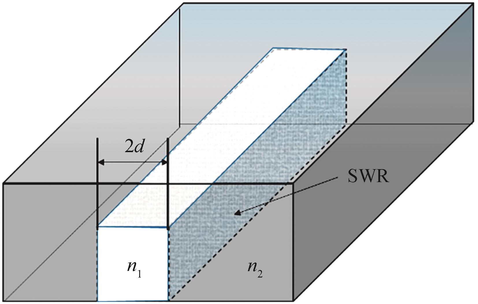
    Fig. 1 shows a schematic 3-D configuration of a straight waveguide in which the waveguide core has a refractive index of n1 and a channel width of 2d , and the cladding material has a refractive index of n2, and the effective index of the guided-mode is Neff. If the wavelength of the light wave in air is λ, with the wave number k0=2π/λ and the Finite Difference Processing of Beam Propagation Method (FD-BPM), the effective index Neff of a single guided-mode is obtained, and further based on the propagation constant of this guided-mode β=k0Neff, three dimensionless parameters hV and p of guided-mode defined by the PL model can be defined as 3-4

    h,V,p=dn12k02-β2,k0dn12-n22,dβ2-n22k02

    Perspective view of a schematic SOI waveguide

    Figure 1.Perspective view of a schematic SOI waveguide

    where h and p are the parameters defining the guided mode field in the literature on optical waveguides 1112V is the product of three elements, n12-n22 is the numerical aperture of a symmetric planar waveguide, d is half width of the waveguide core, leading to the other dimensionless parameters as

    Δ,x,γ=(n12-n22)/(2n12),p(Lc/d)p(Lc/d),(n2V)/(n1pΔ)

    Consequently, for both the TE-like and TM-like modes, the SWR induced optical scattering loss is related to both the y- and z-components of roughness, so the dependences of the optical intensity loss coefficients α3D(TE/TM)on the 3-D SWR σ3D(TE/TM) can be expressed as 3

    α3D(TE/TM)=4.34σ3D2(TE/TM)2d4βTE/TMg(V)fe(x,γ)

    where α3D(TE/TM) is the SWR defined in the 2-D form and the loss coefficient is in dB/cm, the functions g(V) is defined as

    g(V)=h2V21+p2

    and fe(x,γ) is defined as

    fe(x,γ)={[(1+x2)2+2x2γ2]1/2+1-x2}1/2[(1+x2)2+2x2γ2]1/2

    where transferring functions, fe(x,γ) is used to determine the correlation length Lc with the parameters x and γ at the peak value.

    1.2 Determination of the Correlation Length Lc

    The numerical simulation for the function fe(x,γ) is shown in Fig. 2, where the peak position indicates the maximum autocorrelation value. So, the corresponding values of x and γ play the role of making fe(x,γ) have the maximum autocorrelation effect, and then the corresponding Lc value calculated from Eq. (2) is the correlation length value of this waveguide.

    2 Numerical simulations of optical propagation loss

    2.1 Numerical simulations for variables x and γ of the function fe(x,γ)

    With Eq. (4), the numerical simulation results of two key variables x and γ of the function are obtained as shown in Figs. 3(a) and 3(b), respectively. From Fig. 3(a), we find that the variable x is strongly dependent on the refractive index of the SOI waveguide core, but it is weakly dependent of the rib width. Illustratively, all the five curves are very close to one another, namely, when the core refractive index is changed from 3.43 to 3.48, almost all the five x values are decreased from 1.691 3 to 1.688 5. For the simulation results of variable γ are almost the same as the case of x. For instance, γ is also weakly dependent of the rib width, so all the five curves are very close to one another, namely, when the core refractive index is changed from 3.43 to 3.48, almost all the five γ values are decreased from 0.673 to 0.662. The comparison between Figs. 3(a) and 3(b) also shows that corresponding to the effective index change, the relative change of x is only 0.17%, while the relative change of γ reaches 1.63%. In summary, γ has the much stronger dependence on the refractive index of SOI waveguide core than x, but they are almost independent of the rib width.

    2.2 Numerical simulations for the correlation length Lc on the waveguide structure

    With the simulation results of x and γ shown in Figs. 3(a) and 3(b), respectively, with Eq. (4), the plot of function fe(x,γ) versus variable x for each waveguide structure is carried out and then the value of the correlation length Lc of this waveguide structure is obtained. Further, for the possible waveguide structures that can create single-mode operations, the corresponding distributions of Lc are obtained with respect to five values of channel width Wr as shown in Fig. 4.

    Note that the dependences of Lc on the two waveguide parameters: the rib width and the core refractive index are inverse to the cases of the two variables x and γ. Namely, Lc has no big change with the core refractive index, but all the five lines of Lc values are dramatically different from one another, namely, it strongly dependent on the rib width of the SOI waveguide. Eqs. (1) ~ (3) show that the OPL coefficient α3D is related to both Lc and Wr (i.e., 2d), so these two parameters of waveguide: n1 and 2d have great impacts upon the SWR-caused OPL.

    3 Measurements for the anisotropic SWR and the OPL

    3.1 Measurements for the SWR distributions of SOI waveguides

    With the fabricated device sample, the reconstructed images of CLSM measurements for an SOI waveguide sidewall roughness could further be obtained. During measuring the SWR distributions, the chip of SOI waveguides is rotated by a quasi-90° angle and then measured the sidewall profile of the waveguide with CLSM. As a result, the average horizontal and the average vertical values of SWR are 22 nm and 23 nm, respectively. As defined in our previous work, the SWR values at both TE- and TM-mode are measured. In this definition of roughness, the PSz, which is given by the CLSM measurement in unit of μm, indicates the average roughness value in the scanned range of CLSM measurement and it can be taken as a one-dimensional (1-D) roughness σ(1a), then the 2-D average roughness σ2D(2a) and the 3-D average roughness σ3D(3a) are defined as 3

    σiso(2D)=(1/m)j=1mPSz

    σani(3D)=(1/n)j=1nσiso(2D)

    For the waveguide structure of fabricated device sample, with the theoretical model defined by Eqs. (1)~(7), the dependences of OPL coefficient on the SWR for both TE- and TM-mode are simulated as shown in Fig. 5. Note that the OPL coefficient caused by the SWR quickly increases with SWR and the TE-mode always bigger than the TM-mode. For instance, at the above measured values, 22 nm and 23 nm for the horizontal and vertical distributions, the OPL values for both the TE- and TM-mode are 5.0 dB/cm. So, a high-quality SOI waveguide, the SWR should be controlled lower than 20 nm. In addition, the difference of the OPL values between the TE- and TM-mode also quickly increases.

    Numerical simulations for the OPL coefficient α3D vs SWR of SOI waveguide for TE- and TM-mode

    Figure 5.Numerical simulations for the OPL coefficient α3D vs SWR of SOI waveguide for TE- and TM-mode

    In experiments for verifying the mean OPL value, the two ends of the waveguide chip are polished to form a Fabry-Perot (F-P) cavity. Then, a response of the optical resonance output to the temperature change is obtained as shown in Fig. 6. Since the F-P response curve to temperature change contains two wave periods, so, as labelled in Fig. 6, two periods: Period-1 and Period-2 are used to calculate the OPL values with the popular format as defined by Eq. (8)13.

    α=4.34lwgln1-Tmin/Tmax1+Tmin/TmaxNeff+1Neff-12

    Propagation losses test of three SOI waveguides and the responses of F-P cavity formed by the waveguide channel to temperature change

    Figure 6.Propagation losses test of three SOI waveguides and the responses of F-P cavity formed by the waveguide channel to temperature change

    where lwg represents the length of the waveguide 11, and Tmax and Tmin represent the maximum and minimum values of transmission of resonance curve. Consequently, the OPL values are obtained to be 4.218 4 and 4.312 5 dB/cm for the two periods, leading to an average OPL value of 4.265 dB/cm. This result agrees with the calculated values in Fig. 5 for either TE-mode or TM-mode. Nevertheless, compared with the measured values of the similar scaled SOI waveguides in literature published by VLASOV V A et al. in 2002 and BOEUF F et al. in 2016 1415, the measured results obtained in this article are higher than the high-quality SOI waveguides should have. So, the fabrication technique for the samples used in this work still needs to be improved.

    4 Conclusion

    As a conclusion, through self-consistent modeling and numerical simulations of the two key factors in the guided mode of an SOI waveguide: the correlation length and the SWR, the ideal simulation results are obtained. Based on the research on the surface roughness of SOI waveguides, we can introduce the 3-D distribution of SWR and the interaction effect between the optical field of guided mode and the SWR to create accurate theoretical model for defining the optical loss coefficient dependence on the waveguide structure and SWR.

    References

    [1] H YNAMAZAKI, T SAIDA et al. Dual carrier dual-polarization IQ modulator using complementary frequency shifter. IEEE Selected Topics on Quantum Electronics, 19, 3400208(2013).

    [2] A S LIU, R JOHNS, L LIAO et al. A high-speed silicon optical modulator based on a metal-oxide-semiconductor capacitor. Nature, 427, 615-620(2004).

    [3] H P SHANG, D G SUN, P YU et al. Investigation for sidewall roughness caused optical scattering loss of silicon-on-insulator waveguides with confocal laser scanning microscopy. Coatings, 10, 236(2020).

    [4] F P PAYNE, J P R LACEY. A theoretical analysis of scattering loss from planar optical waveguides. Optical and Quantum Electronics, 26, 977-986(1994).

    [5] T BARWICZ, H A HAUS. Three-dimensional analysis of scattering loss due to sidewall roughness in micro photonic waveguides. IEEE Lightwwave Technology, 23, 2719-2732(2005).

    [6] C G POULTON, C KOOS, M FUJII et al. Radiation models and roughness loss in high index-contrast waveguides. IEEE Selected Topics on Quantum Electronics, 12, 1306-1321(2007).

    [7] J H SCHMID, A DELÂGE, B LAMONTAGNE et al. Interference effect in scattering loss of high-index-contrast planar waveguides caused by boundary reflections. Optics Letters, 33, 1479-1481(2008).

    [8] A DELÂGE, J LAPOINTE et al. Correlation of scattering loss, sidewall roughness and waveguide width in silicon-on-insulator (SOI) ridge waveguides. IEEE Journal of Lightwave Technology, 27, 3999-4008(2009).

    [9] D G SUN, H P SHANG, H L JIANG et al. Effective metrology and standard of the surface roughness of micro/nanoscale waveguides with confocal laser scanning microscopy. Optics Letters, 44, 747-750(2019).

    [10] H P SHANG, D G SUN, Q Y SUN et al. Analysis for system errors in measuring sidewall angle of silica waveguides with confocal laser scanning microscope (CLSM). Measurement Science and Technology, 30, 025004(2019).

    [11] C R DOERR, K OKAMOTO. Planar lightwave circuits in fiber-optic communications. Optical Fiber Telecommunications, 269-341(2008).

    [12] E J MURPHY. Optical circuits and components: design and applications(1999).

    [13] C FEUCHTER T THIRSTRUP. High precision planar waveguide propagation loss measurement technique using a Fabry-Perot cavity. IEEE Photonics Technology Letters, 6, 1244-1247(1994).

    [14] V A VLASOV, S J MCNAB. Losses in single-mode silicon-on-insulator strip waveguides and bends. Optics Express, 12, 1622-1631(2004).

    [15] F BOEUF, S CREMER, E TEMPORITI. Silicon photonic R&D and manufacturing on 300-mm wafer platform. IEEE Lightwave Technology, 33, 286-295(2016).

    Bin WANG, Degui SUN, Hongpeng SHANG. Investigation for Relationship between Sidewall Roughness of Silicon-on-insulator Waveguide and Loss of Guided-mode[J]. Acta Photonica Sinica, 2021, 50(5): 151
    Download Citation