Abstract
We have designed and fabricated zero-bias operational two-element symmetric-connected photodetector arrays (SC-PDAs). The designed SC-PDAs have higher saturation currents, larger RF power, and better frequency responses than the single photodetector (PD) under zero bias. The bias-free SC-PDA with 15 μm diameter of each PD demonstrated a 3 dB bandwidth of 19.4 GHz at 0.5 mA. The RF saturation photocurrent and maximum RF output power of the SC-PDA with 40 μm, 50 μm, and 60 μm diameters under zero bias are over 9.31 mA and ?5.86 dBm at 3 GHz, 14.52 mA and 1.17 dBm at 1 GHz, and 13.72 mA and ?1.76 dBm at 1 GHz, respectively.With the demand for large capacity communication and high data rate transmission increasing ever since, developing the next generation of high symbol rate wired fiber communication, photonic millimeter-wave wireless communication system, and optical interconnection network is very urgent and necessary. High power and high speed photodetectors (PDs) play a key role in such optical receivers, as well as the photonic oscillator[1] for millimeter-wave generating, because of its high dynamic range and low noise compared to the electric oscillator[2,3]. For the high speed design, the PD should be designed with a small active area and a thin absorption layer to maintain a low junction capacitance and a short transit time[4]. But, the smaller active area will cause a high photocurrent density, which will affect the saturation performance due to the space charge effect[5]. In addition, a small diameter device will cause a thermal failure at high operational photocurrent. So, it is difficult to guarantee a high saturation output power and a high 3 dB bandwidth at the same time. In order to overcome this contradiction, different epitaxy structure designs are proposed, including the uni-traveling carrier PD (UTC-PD)[6], greatly reducing the limitation of the space charge effect on the device performance. Some modifications of UTC-PD are put forward, such as adding a high-concentration-doped cliff layer[7], and reasonable design of the thickness and doping concentration of the collection layer[3,8], to further improve the high speed and high power performance. But, the thermal stress is also a great limitation.
The distributed PD array has been developed[5,9–12], in which the optical signal is fed into several PDs, and their photocurrent is combined by a transmission line. In this way, every single PD could operate effectively out of the thermal failure, and the PD array can achieve a high power output at the same time. The hybrid integrated traveling-wave photodiode array (TWPDA)[5] with a high saturation current of 114 mA and electrical output power up to 13 dBm is obtained. But, the different electric transmission length of each PD[5,10] could result in a phase mismatch. Our group demonstrated the two-element symmetric-connected photodetector (SC-PDA), in which every single PD has an equivalent electrical propagation length for eliminating the phase mismatch. A saturation current of 87.9 mA and a maximum output RF power of 16 dBm of the SC-PDA are obtained[10–11]. But, those kinds of arrays need external bias circuit support and operate at a quite high bias voltage of more than 3 V. Actually, in the photonic wireless communication network, every access network is a distributed cell. It is necessary to reduce the connected cable equipment and the power consumption of each unit[3]. In addition, shrinking the footprints to achieve a more compact receiver is very important. Although the high bias voltage could compensate the space charge effect of the PD, the thermal stress is increased, and the crosstalk is more awful with amounts of external bias circuits in the high density integrated photonic system.
In this study, we proposed and fabricated a zero-bias operational two-element SC-PDA with an optimized UTC-PD epitaxial structure to eliminate the additional external bias circuit and compensate the output power of the single zero-bias photodiode. The different diameter scale SC-PDAs with the same epitaxial structure were fabricated. The frequency response and saturation performance of the PDs without bias and under a low bias of no more than 2 V were tested, respectively.
Sign up for Chinese Optics Letters TOC. Get the latest issue of Chinese Optics Letters delivered right to you!Sign up now
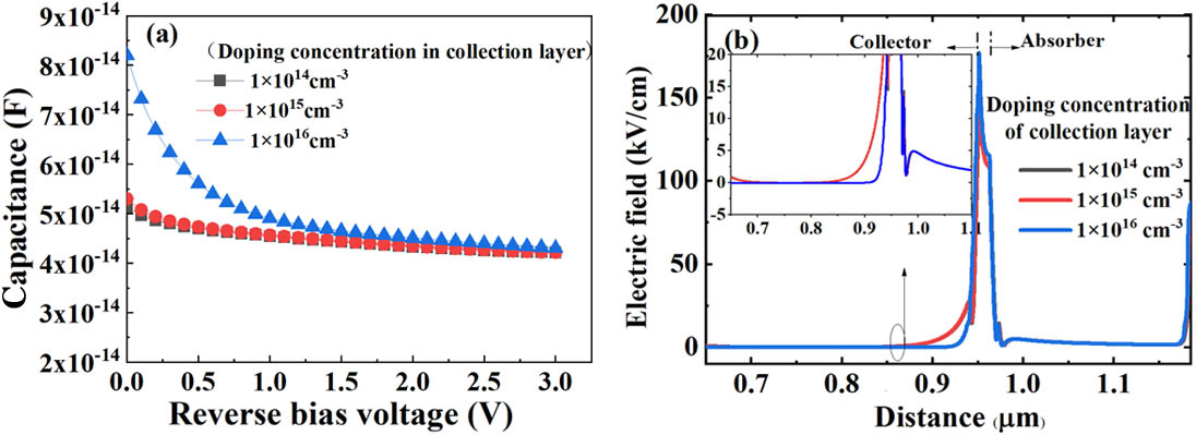
The modified UTC-PD is designed with the motivation of increasing the 3 dB bandwidth and the maximum saturation photocurrent under zero bias. The absorption layer thickness and the carrier collection thickness, which affect the PN junction capacitance, are very important for achieving zero-bias operation. The optimized epitaxial structure for high speed response at zero bias is evolved from the device described in our previous work[12]. In this study, the absorption layer is in the graded-doped range from to with the thickness decreasing to 220 nm to shorten the transit time and keep the responsivity not too small at the same time. The thickness of the collection layer was selected as 350 nm to make the junction capacitance and the transit time reach a compromise. The highly-doped collection layer in Ref. [12] cannot be depleted completely at low bias voltage. At this time, the junction capacitance will be large, and the electric field of the collection layer will be quite low, which is not conducive to the transport of carriers. The doping concentration of the collection layer should be as low as possible to ensure the device could operate at zero bias or a low bias voltage[3,13–16]. However, a technical issue regarding the epitaxial growth process cannot guarantee an extremely lowly-doped N-type layer or an undoping epitaxial layer in the growth process, which has the risk of PN reversal[13]. So, the influence of the different doping concentration in the collection layer on the device was simulated before the epitaxial growth. Figure 1(a) shows the capacitance-voltage curve of a single 15 μm diameter UTC-PD with different doping concentrations in the collection layer. The device that is highly-doped () in the collection layer has a higher capacitance when the reverse bias voltage below 1.5 V is compared with the low doping concentration ( and ) ones. The PD is fully depleted when the reverse bias voltage is above 2 V. There is no obvious difference on the capacitance and electric field when the doping concentration is and . Considering the limitation of the doping process, the doping concentration of the collection layer is confirmed as .

Figure 1.(a) Capacitance-voltage characteristics of the UTC-PD with different doping concentrations in the collection layer. (b) The electric field distribution of the UTC-PD with the different doping concentrations in the collection layer under zero bias.
The included lightly doped () is inserted into the space layer to reduce the conduction band offset of InP and InGaAs. The P-type highly-doped is the carrier blocking layer. The highly P-doped InGaAs and N-doped InP is the contact layer for good ohmic contact with the metal pad. Finally, the epitaxial structure is as Table 1 demonstrates.
| Material | Doping (cm−3) | Thickness (nm) | Layer |
|---|
| P‐In0.53Ga0.47As | 2×10¹⁹ | 50 | P-contact layer |
| P‐In0.77Ga0.23As0.499P0.501 | 1×10¹⁹ | 20 | Blocking layer |
| P‐In0.53Ga0.47As | Graded-doped | 220 | Absorber |
| P‐In0.53Ga0.47As | 1.5×10¹⁸ | 10 | Spacer1 |
| N‐In0.77Ga0.23As0.499P0.501 | 1×10¹⁵ | 12 | Spacer2 |
| N-InP | 1.5×10¹⁸ | 10 | Spacer3 |
| I-InP | <1×10¹⁵ | 350 | Collector |
| N-InP | 1×10¹⁷ | 50 | Sub-collector |
| N‐In0.77Ga0.23As0.499P0.501 | 1×10¹⁸ | 15 | Etch stop layer |
| N-InP | >1×10¹⁹ | 500 | N-contact layer |
Table 1. Epitaxial Structure of the UTC-PD
The PD elements of the SC-PDA with the epitaxial structure in Table 1 are grown on a semi-insulating (S.I.)-InP substrate. Commercial PD chips at 1550 nm typically have active diameters ranging from 50 to 70 μm for sufficient light coupling from an optical multimode fiber with a 50 μm core diameter. The large active area benefits from reduced coupling loss and relaxed alignment tolerances. But, for the high speed application, the small area can largely reduce the resistor–capacitor (RC)-limited bandwidth. For different application, the PD mesa ranges from 15 μm to 60 μm are fabricated.
The cylindrical mesa structures of the PD elements were fabricated with standard semiconductor fabrication processes including photolithography, wet chemical etching, and magnetron sputtering of the contact electrodes. The Ti/Au (60 nm/300 nm) was deposited on the P-contact InGaAs layer and patterned by the lift-off process to form the circular mesa structure. The InGaAs, InGaAsP, and InP layers were etched by , and several times to form the N-type InP contact layer. After that, the (230 nm) was deposited on the N-contact layer by magnetron sputtering and then annealed with the temperature ranging from 100°C to 420°C around nitrogen ambient for low ohmic contact resistance. After the photodiode mesas and contact electrodes were formed, a layer of polyimide was spin-coated on the wafer as a passive layer and annealed for pre-passivation in nitrogen ambient. The top window was opened to ensure the connection between the N-electrode and the ground pad. After that, the coplanar waveguide (CPW) transmission lines and the ground pad were evaporated on top of the passive layer to connect the PD elements. The experiment result shows that the electrodes have good ohmic contact and stability performance. The configuration of the two-element array still adopts symmetrical connection ways that we proposed previously in Ref. [12]. But, the transmission loss is reduced by 1.1 dB at 40 GHz by optimizing the length and width of the CPW transmission line to 76 μm and 40 μm, which connect the detector P-electrode to the central conductor. The width of the center conductor and the gap between the center conductor and ground pad are 85 μm and 45 μm, respectively. The spacing of the adjacent detectors is still designed as 250 μm for the two optical fibers to have enough space to move and adjust the relative position during the test. The detailed design and experimental results of the optimized SC-PDA electrodes can be found in our previous work, see Ref. [17]. The micrograph of the fabricated SC-PDA is shown in the inset of Fig. 2.
Figure 2.Schematic experiment setup of the (a) frequency response and (b) RF output power. The inserted figure is the micrograph of the fabricated SC-PDA with 15 μm diameter of each PD.
The fabricated SC-PDA was tested on the wafer. The photocurrent and RF output signal of the device were collected by the GSG150 microwave probe and monitored in time by the Keithley source meter and the microwave power meter through the RF path of the bias-tee, respectively, and a reverse bias voltage is applied through DC path. The optical power fed into the PDs is implemented by two lensed fiber probes. An optical power splitter is used to divide the optical power to put into the two lensed fibers. The dark current of the SC-PDA with different diameters was tested, as shown in Fig. 3(a). It is noted that a larger diameter of each PD and a higher reverse bias voltage will cause a larger dark current. The dark current of the SC-PDA with a diameter of 15 μm less than 4 nA is obtained when the reverse bias voltage is less than 2 V.
Figure 3.(a) Measured dark current of the SC-PDA versus the PD diameter. (b) Measured DC response of the fabricated SC-PDA, the SC-PDA in Ref. [12], and the corresponding single PD element. The data were measured with 1550 nm incident light without bias.
The DC characteristics of the 60 μm diameter device without bias are demonstrated in Fig. 3(b). The single PD element was tested by moving one of the lensed fibers away from the other PD. The SC-PDA we fabricated previously in Ref. [12], which has a graded-doped 600 nm absorption layer and a 400 nm collection layer with the doping concentration of in the collection layer, was tested, and the responsivity of the single PD element of the SC-PDA[12] is about 0.375 A/W. The DC saturation photocurrent of the SC-PDA is about 10 mA at zero bias when both PD elements receive optical power. By comparison, the single PD-element responsivity of the designed zero-bias operational SC-PDA is 0.226 A/W. The high photocurrent of the designed SC-PDA over 52 mA is observed without DC saturation at zero bias. Both results are almost twice that of the corresponding single PD. In contrast, the decrease of responsivity is due to the decrease of the thickness of the absorption layer. But, with the low doping and proper thickness of the collection layer, the designed SC-PDA has a higher DC saturation photocurrent under the zero-bias voltage.
The small signal frequency response was tested by a tunable laser and an Agilent E8363C network analyzer in a range from 10 MHz to 40 GHz; the schematic experiment setup is shown as Fig. 2(a). The calibration of the phase of the two optical path signals was done by aligning both fibers to a large area single photodiode and by adjusting one lensed fiber vertically if the phase difference is small, or a delay line in one optical path can be used when there is a quite large phase difference until the coherent subtraction measured at the output pad disappears[11]. The frequency response of the SC-PDA with the PD-element diameter of 15 μm was tested when both PD elements received optical power at reverse bias voltages of 0 V, 1 V, and 2 V under a photocurrent of 0.5 mA. As Fig. 4 plots, the 3 dB bandwidth of the SC-PDA reaches 19.4 GHz and 24.2 GHz at a reverse bias voltage of 0 V and 1 V, respectively. As the reverse bias voltage increases to 2 V, the frequency response no longer performs an obvious raise compared with 1 V, which indicates that the device is already depleted completely when the reverse bias is below 2 V. The depleted reverse bias voltage is consistent with our simulation. Besides, the frequency responses of different-diameter SC-PDA single PD with the same designed epitaxial structure and the reported SC-PDA[12] have been tested similarly.
Figure 4.Measured frequency response of the fabricated SC-PDA with the 15 μm diameter PD elements at 500 μA photocurrent.
The 3 dB bandwidth versus the diameter is shown as Fig. 5. The 3 dB bandwidth of the designed SC-PDA with a diameter of 20 μm, 40 μm, 50 μm, and 60 μm is 6 GHz, 3.1 GHz, 1.1 GHz, and 0.9 GHz, respectively, under 1 mA photocurrent without bias. There is a great increase compared with the reported SC-PDA[12] with the same active area. It accounts for the thickness decrease of the absorption layer and the low doping in the collection layer. With the increase of the PD diameter from 15 μm to 20 μm, the 3 dB bandwidth of the SC-PDA at 0 V is decreased abruptly, but with the PD diameter increase from 20 μm to 60 μm, the slope of the 3 dB bandwidth versus PD diameter curve becomes smaller, which is similar to the report in Ref. [18]. The 3 dB bandwidth of the single PD with a diameter of 20 μm, 40 μm, 50 μm, and 60 μm is 13.3 GHz, 6.6 GHz, 1.6 GHz, and 1.2 GHz, respectively, under 1 mA photocurrent without bias. When the diameter of the PD element is more than 40 μm, the 3 dB bandwidth between the SC-PDA and single PD becomes comparable at 0 V. It is noted that the 3 dB bandwidth is RC-limited due to the thin absorber and large active area. So, to find the reasons for the 3 dB bandwidth behavior, the capacitance of different-diameter PDs is extracted from the measured scattering parameters of microwave reflection coefficients (). As Fig. 6 plots, the capacitance is going down when the testing RF frequency increases. When the diameter of the PD increases, the slope of the capacitance versus the PD diameter curve becomes smaller as the RF frequency is below 20 GHz. So, the slope of the 3 dB bandwidth versus the PD diameter curve becomes smaller when the diameter increases. The capacitance of the SC-PDA is almost twice that of the single PD due to the electric parallel-connected ways. But, when the diameter of the PD is more than 40 μm, the RC-limited bandwidth becomes relatively small under zero bias due to the large capacitance. The 3 dB bandwidth of the SC-PDA is comparable to the single PD when the diameter of the PD element is more than 40 μm. The measured small signal frequency response of the SC-PDA and the corresponding single PD element with 50 μm diameter at 0 V bias and a photocurrent of 2 mA is plotted in Fig. 7. The 3 dB bandwidth of SC-PDA is comparable to the single ones, but the RF output power is almost equal to the sum of the two single PD elements. (The RF output power of SC-PDA has almost a 3 dB rise compared with the single one.) The large size SC-PDA could compensate the RF output power of the single PD without sacrificing much of the 3 dB bandwidth under 0 V. This characterization of the large size zero-bias SC-PDA is impressive and has a great potential for high power and large coupling tolerance applications.
Figure 5.Measured 3 dB bandwidth versus different diameters of the PD elements under zero bias at 1 mA photocurrent.
Figure 6.Measured capacitance of the fabricated SC-PDA and the corresponding single PD element with different diameters without bias at 1 mA photocurrent. The inserted figure is the capacitance versus different diameter of the PD when the RF frequency is 10 GHz.
Figure 7.Measured small signal frequency response of the SC-PDA and PD elements with a diameter of 50 μm at 0 V bias and a photocurrent of 2 mA.
The photocurrent dependent RF output power of the different-diameter SC-PDA was tested by the microwave power meter, as shown in Fig. 2(b). The optical heterodyne setup can provide a modulation depth close to 100%. The SC-PDAs with diameters of 40 μm, 50 μm, and 60 μm at zero-bias operation have a saturation photocurrent and corresponding maximum RF output power exceeding 9.31 mA and at 3 GHz, 14.52 mA and 1.17 dBm at 1 GHz, and 13.72 mA and at 1 GHz, respectively, as demonstrated in Fig. 8(a). Those results are the highest in the PDs with the comparable active area under zero bias as we know. For the SC-PDA with a diameter of 50 μm, with the increase of reverse bias voltage, the RF output keeps increasing at the same photocurrent until the bias is up to 3 V. The higher bias hardly affects the output RF power. When the reverse bias voltage is 3 V, the saturated output exceeds 15.0 mA and 12.12 dBm, as Fig. 8(b) shows.
Figure 8.(a) Measured RF output power versus photocurrent of different-diameter SC-PDA under zero bias. (b) Measured RF output power versus photocurrent of 50 μm diameter SC-PDA under different reverse bias voltage.
In conclusion, the two-element bias-free SC-PDA with different diameters ranging from 15 μm to 60 μm is proposed and fabricated for eliminating the external bias circuit and compensating the output power of the single zero-bias photodiode. The back-illuminated SC-PDA and the single PD element with the same UTC-PD epitaxial structure were tested. The designed SC-PDA with large diameter can compensate the output power of single PD but almost does not sacrifice the 3 dB bandwidth under zero bias. The proposed device demonstrates higher power handling capability than the single PD under zero-bias voltage. To further improve the high power and high speed performance under zero bias, the photodiode element could be designed with a smaller diameter. For optimizing the footprint of the chip, the thermal stress, and the coupling tolerance, the proposed large area zero-bias photodiode arrays have a great potential for high power and high speed applications.
References
[1] Y. Xu, H. Peng, R. Guo, H. Du, G. Hu, L. Zhu, Z. Chen. Chin. Opt. Lett., 16, 110602(2018).
[2] T. M. Fortier, M. S. Kirchner, F. Quinlan, J. Taylor, J. C. Bergquist, T. Rosenband, N. Lemke, A. Ludlow, Y. Jiang, C. W. Oates, S. A. Diddams. Nat. Photon., 5, 425(2011).
[3] T. Umezawa, A. Kanno, K. Kashima, A. Matsumoto, K. Akahane, N. Yamamoto, T. Kawanishi. J. Lightwave Technol., 34, 3138(2016).
[4] T. Liu, Y. Huang, J. Fei, G. Wu, X. Ma, X. Duan, K. Liu, X. Ren. Chin. Opt. Lett., 16, 051301(2018).
[5] A. Beling, H. Chen, H. Pan, J. C. Campbell. IEEE Photon. Technol. Lett., 21, 1813(2009).
[6] T. Ishibashi, N. Shimizu, S. Kodama, H. Ito, T. Nagatsuma, T. Furuta. Ultrafast Electronics and Optoelectronics, UC3(1997).
[7] Z. Li, H. Pan, H. Chen, A. Beling, J. Campbell. IEEE J. Quantum Electron., 46, 626(2010).
[8] T. Umezawa, A. Kanno, K. Akahane, A. Matsumoto, N. Yamamoto, T. Kawanishi. Proc. SPIE, 10531, 1053115(2018).
[9] P. Runge, F. Ganzer, T. Beckerwerth, S. Keyvaninia, S. Mutschall, A. Seeger, W. Ebert, M. Schell. IEEE Photon. Technol. Lett., 31, 246(2019).
[10] A. S. Cross, Q. Zhou, A. Beling, Y. Fu, J. C. Campbell. Opt. Express, 21, 9967(2013).
[11] J. Fei, Y. Huang, T. Liu, X. Ma, X. Duan, K. Liu, X. Ren. IEEE Photon. Technol. Lett., 29, 1627(2017).
[12] J. Fei, Y. Huang, W. Fang, T. Liu, X. Duan, K. Liu, X. Ren. Opt. Express, 25, 21726(2017).
[13] T. Umezawa, K. Akahane, N. Yamamoto, A. Kanno, K. Inagaki, T. Kawanishi. Optical Fiber Communications Conference and Exhibition, M3C.7(2015).
[14] W. Liu, R. Cendejas, H. Cao, Q. Hang, Z. Ji, A. Nikolov. CLEO: Science and Innovations, CTh3L.2(2013).
[15] Q. Yu, Z. Wang, K. Sun, F. Yu, J. Zang, J. C. Campbell, A. Beling. IEEE Photonics Conference, 1(2018).
[16] T. Liu, Y. Huang, H. Niu, J. Fei, X. Ma, G. Wu, K. Liu, X. Duan, X. Ren. Opt. Quantum Electron., 50, 284(2018).
[17] K. Zhao, Y. Huang, J. Fei, X. Duan, K. Liu, X. Ren. Asia Communications and Photonics Conference, Su2A.123(2017).
[18] R. Sankaralingam, P. Fay. IEEE Photon. Technol. Lett., 17, 1513(2005).