• Photonics Research
  • Vol. 8, Issue 6, 858 (2020)
J. Hawecker1、*, V. Pistore1, A. Minasyan2, K. Maussang1、4, J. Palomo1, I. Sagnes3, J.-M. Manceau3, R. Colombelli3, J. Tignon1, J. Mangeney1, and S. S. Dhillon1
Author Affiliations
  • 1Laboratoire de Physique de l’Ecole normale supérieure, ENS, Université PSL, CNRS, Sorbonne Université, Université de Paris, F-75005 Paris, France
  • 2i2S, 28-30 rue Jean Perrin 33608 Pessac, France
  • 3Centre de Nanosciences et de Nanotechnologies (C2N), CNRS UMR 9001, Université Paris-Saclay, 91120 Palaiseau, France
  • 4Currently at: Institut d’Electronique et des Systèmes, CNRS (UMR 5214), Univ Montpellier, 860 rue de Saint-Priest, 34 095 Montpellier Cedex 5, France
  • show less
    DOI: 10.1364/PRJ.388219 Cite this Article Set citation alerts
    J. Hawecker, V. Pistore, A. Minasyan, K. Maussang, J. Palomo, I. Sagnes, J.-M. Manceau, R. Colombelli, J. Tignon, J. Mangeney, S. S. Dhillon. Cavity-based photoconductive sources for real-time terahertz imaging[J]. Photonics Research, 2020, 8(6): 858 Copy Citation Text show less
    (a) Schematic of the standard quasi-cavity structure. (b) Interdigitated switch. (c) Enhanced view of the latter. The quasi-cavity structure has a buried metal plane a few micrometers, d, below the surface of the interdigitated structure.
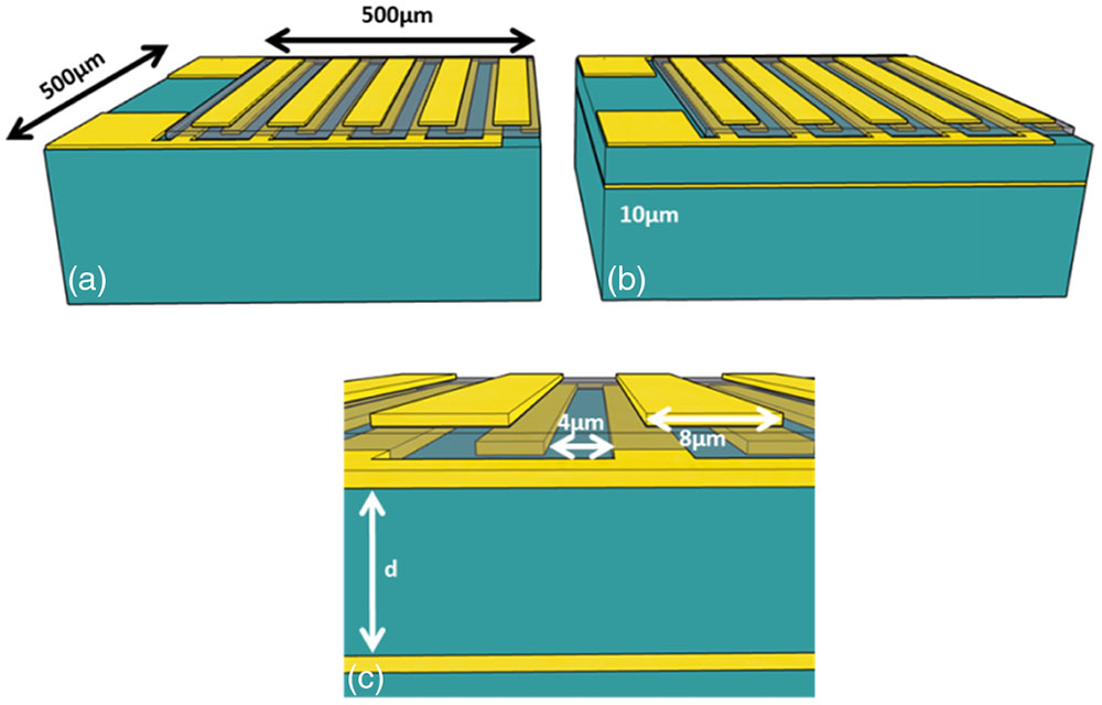
    Fig. 1. (a) Schematic of the standard quasi-cavity structure. (b) Interdigitated switch. (c) Enhanced view of the latter. The quasi-cavity structure has a buried metal plane a few micrometers, d, below the surface of the interdigitated structure.
    Electromagnetic simulations of the x polarized emitted electric field at 1 and 1.5 THz (maximum field emission of the standard and quasi-cavity PC switch, respectively) for the (a), (b) quasi-cavity and (c), (d) standard PC switch.
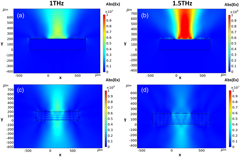
    Fig. 2. Electromagnetic simulations of the x polarized emitted electric field at 1 and 1.5 THz (maximum field emission of the standard and quasi-cavity PC switch, respectively) for the (a), (b) quasi-cavity and (c), (d) standard PC switch.
    2D plot of the simulated electric field as a function frequency (y axis) and GaAs active thickness d (x axis). The black solid line corresponds to the quarter wavelength condition with a refractive index of 3.6.
    Fig. 3. 2D plot of the simulated electric field as a function frequency (y axis) and GaAs active thickness d (x axis). The black solid line corresponds to the quarter wavelength condition with a refractive index of 3.6.
    Normalized experimental (black) and simulated (red) spectral response of the quasi-cavity structure. Inset shows the measured time trace.
    Fig. 4. Normalized experimental (black) and simulated (red) spectral response of the quasi-cavity structure. Inset shows the measured time trace.
    (a) Time response of electric fields and (b) spectrum of standard and quasi-cavity-based PC switches.
    Fig. 5. (a) Time response of electric fields and (b) spectrum of standard and quasi-cavity-based PC switches.
    Average power as a function of the applied field for standard (red) and quasi-cavity (black) PC switch.
    Fig. 6. Average power as a function of the applied field for standard (red) and quasi-cavity (black) PC switch.
    2D plot of electromagnetic field distribution for the standard structure with (a) 2 μm and (b) 4 μm interdigit spacing.
    Fig. 7. 2D plot of electromagnetic field distribution for the standard structure with (a) 2 μm and (b) 4 μm interdigit spacing.
    (a) Optical image (front) of the object. (b) Optical image (back of object) of hidden text. (c) Real-time image from the THz camera using the high average power from the quasi-cavity PC switch showing the hidden text. A real-time video is shown in Visualization 1.
    Fig. 8. (a) Optical image (front) of the object. (b) Optical image (back of object) of hidden text. (c) Real-time image from the THz camera using the high average power from the quasi-cavity PC switch showing the hidden text. A real-time video is shown in Visualization 1.
    Schematic of real-time imaging setup. The PC switch is excited by an 800 nm IR beam passing through a hole in the first parabolic mirror. The object to be imaged is placed just after the second parabolic mirror. IR filters ensure that no IR radiation is incident on the camera.
    Fig. 9. Schematic of real-time imaging setup. The PC switch is excited by an 800 nm IR beam passing through a hole in the first parabolic mirror. The object to be imaged is placed just after the second parabolic mirror. IR filters ensure that no IR radiation is incident on the camera.
    J. Hawecker, V. Pistore, A. Minasyan, K. Maussang, J. Palomo, I. Sagnes, J.-M. Manceau, R. Colombelli, J. Tignon, J. Mangeney, S. S. Dhillon. Cavity-based photoconductive sources for real-time terahertz imaging[J]. Photonics Research, 2020, 8(6): 858
    Download Citation