J. Hawecker1,*, V. Pistore1, A. Minasyan2, K. Maussang1,4..., J. Palomo1, I. Sagnes3, J.-M. Manceau3, R. Colombelli3, J. Tignon1, J. Mangeney1 and S. S. Dhillon1|Show fewer author(s)
Author Affiliations
1Laboratoire de Physique de l’Ecole normale supérieure, ENS, Université PSL, CNRS, Sorbonne Université, Université de Paris, F-75005 Paris, France2i2S, 28-30 rue Jean Perrin 33608 Pessac, France3Centre de Nanosciences et de Nanotechnologies (C2N), CNRS UMR 9001, Université Paris-Saclay, 91120 Palaiseau, France4Currently at: Institut d’Electronique et des Systèmes, CNRS (UMR 5214), Univ Montpellier, 860 rue de Saint-Priest, 34 095 Montpellier Cedex 5, Franceshow less
Abstract
Optically driven photoconductive switches are one of the predominant sources currently used in terahertz imaging systems. However, owing to their low average powers, only raster-based images can be taken, resulting in slow acquisition. In this work, we show that by placing a photoconductive switch within a cavity, we are able to generate absolute average THz powers of 181 μW with the frequency of the THz emission centered at 1.5 THz—specifications ideally adapted to applications such as non-destructive imaging. The cavity is based on a metal–insulator–metal structure that permits an enhancement of the average power by almost 1 order of magnitude compared to a standard structure, while conserving a broadband spectral response. We demonstrate proof-of-principle real-time imaging using this source, with the broadband spectrum permitting to eliminate strong diffraction artifacts.1. INTRODUCTION
Terahertz (THz) imaging has become an important technique in non-destructive imaging, where THz photons can penetrate optically opaque materials, and it is finding key roles in a range of industrial applications [1]. A crucial technology is based on optically driven photoconductive (PC) switches [2,3] in THz time-domain spectroscopy (TDS) systems. These offer room temperature, spectrally broad operation, low costs, and fast electrical modulation speeds. However, their low average powers (tens of microwatts) have limited their use to inherently slow raster scanning, where the target to be imaged is physically moved to reconstruct the image. Although a variety of techniques can be implemented to increase the acquisition speed [4], no real-time imaging has been demonstrated, limiting applications that require fast imaging. Although high-power quantum cascade lasers have shown the possibility of real-time imaging [5,6], these show important diffraction artefacts and operate at cryogenic temperatures and high THz frequencies (), limiting their applications. Although multiplied electronic sources can reach THz frequencies, their emitted powers drop rapidly beyond a few hundred gigahertz [7]. In this work, we show that by placing a PC switch within a resonant metal–insulator–metal cavity, we are able to generate, with a standard Ti:sapphire oscillator, average THz powers of 181 μW, with the frequency of the THz emission centered at 1.5 THz—specifications ideally adapted to non-destructive testing (NDT). A proof-of-principle demonstration of real-time THz imaging using a commercial microbolometer is shown, with the broadband nature of the THz source eliminating diffraction effects.
PC switches permit the generation of broadband THz pulses. They are based on a femtosecond optical excitation that generates charge carriers in a semiconductor band. These are accelerated by an applied electrical field generating a time-varying current that radiates a short THz pulse (). Typical PC sources emit average THz powers of 100 μW at best [2,8,9]. Although plasmonic-based PCs have reported milliwatt output powers, these sources require electron-beam lithography [10], limiting their industrial takeup, and no real-time imaging has been shown. Here, standard photolithography for a monolithic THz-cavity is used that is inherently adapted to scalability. Furthermore, as THz power measurements are extremely delicate, we show power characterization with an absolute calibrated detector that corroborates the power estimated from the electric field. Compared with a standard source without a cavity, we show a factor of 7.5 increase in the emitted power, in agreement with our simulations that highlight the expected enhancement. We show the application of these cavity-based switches to THz imaging, where a circular scene of 2 cm diameter can be imaged in real time.
2. STRUCTURE
The concept is based on the geometry of our previous work on “echo-less” PC switches [11,12], where similar switches have been used for high-speed raster hyperspectral THz imaging [13]. This showed how a metallic plane buried below a PC structure can increase the spectral resolution of a THz time-domain system by eliminating the THz pulses from propagating into the substrate. However, no measurements have been realized with the absolute power emitted or applied to real-time THz imaging. Here, we maximized the operating parameters in terms of electromagnetic simulations of the cavity for constructive emission, the applied field, and the optical excitation to reach this performance landmark. Figure 1 shows a schematic of the PC switch and a comparison with a classic version. The top surface is based on interdigitated electrode geometry [14,15]. This permits small spacing between the electrodes while preserving a large PC surface area. For the echo-less device, a thin metal plane is inserted between the active GaAs layer and the top surface at a distance to realize the cavity and reflect the generated THz power with no THz field transmitted through the substrate. Since the transient current photogenerated by the optical excitation pulse has its direction fixed by the interdigitated metallic layers, parallel to the buried gold plane, the structure is similar to an optical Fabry–Perot resonator. As previously reported, the lower longitudinal mode satisfies the resonance condition , where is the wavelength in the active layer, and corresponds to the cut-off frequency. This thickness , however, can also be considered as a quasi-quarter wavelength resonator for wavelengths below the cut-off frequency. As discussed subsequently, this resonator also preserves a broadband response. We show clearly that this permits a constructive interference in the far field and enhances the average absolute output powers to the hundreds of microwatt level with a standard oscillator as exciting laser source.
Sign up for Photonics Research TOC. Get the latest issue of Photonics Research delivered right to you!Sign up now
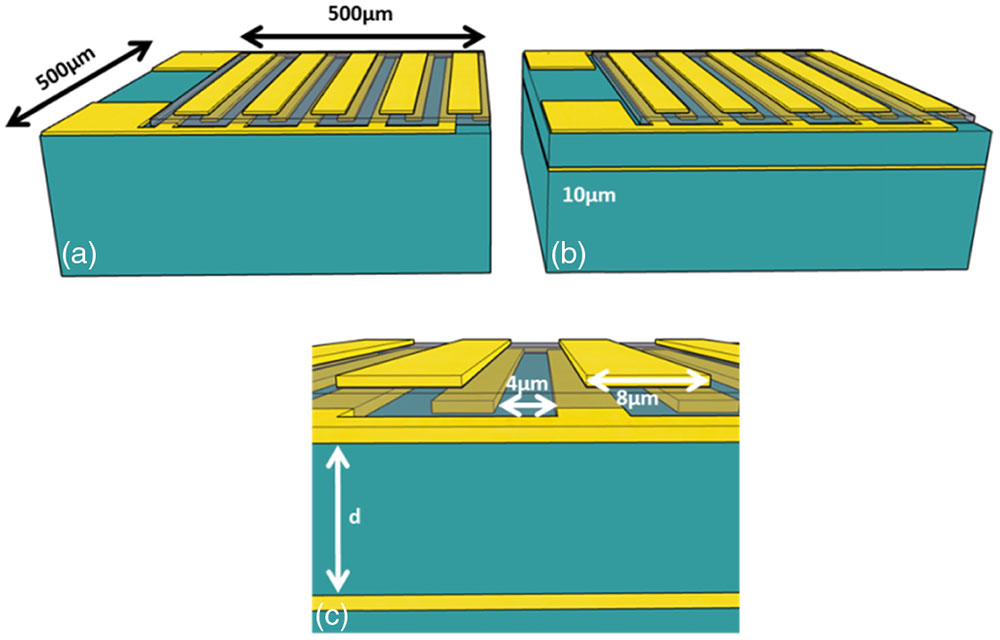
Figure 1.(a) Schematic of the standard quasi-cavity structure. (b) Interdigitated switch. (c) Enhanced view of the latter. The quasi-cavity structure has a buried metal plane a few micrometers, , below the surface of the interdigitated structure.
The processing of the devices is based on a metal wafer bonding technique. The sample was grown by metal organic chemical vapor phase deposition (MOCVD) on a semi-insulating (SI) GaAs wafer with an AlGaAs etch stop layer, followed by the 10 μm thick undoped GaAs active layer. The sample was wafer-bonded to a gold-coated host SI GaAs substrate. The original substrate and the AlGaAs layer were selectively removed, leaving the GaAs active region exposed with a metal plane 10 μm below the surface.
3. NUMERICAL RESULTS
Electromagnetic simulations (COMSOL) of the field from the interdigitated structures are shown in Fig. 2 for a radiated frequency of 1.5 and 1 THz, corresponding to the frequency of highest emission of the quasi-cavity and standard switch, respectively. The interdigitated metal structure (Au) has a digit separation of 4 μm, with 4 μm wide electrodes on a GaAs surface. A dielectric (300 nm ) is placed on top of this structure, allowing for the electrical insulation of the gold fingers from a second metallic digit covering gaps with a periodicity double that of the first (see Fig. 1). This permits optical excitation of every second period of the gaps of the first metallization, and hence excitation of only one bias field direction, preventing destructive interferences of the generated THz far field. The buried metal device in Figs. 2(a) and 2(b) is simulated with a thickness of 10 μm. For comparison, an identical interdigitated structure was also simulated on a 500 μm thick SI GaAs substrate in Figs. 2(c) and 2(d) (i.e., without the buried metal plane). The FDTD simulations were performed using COMSOL Multiphysics. The simulated area was 3 mm in diameter, which corresponds to 5 times the largest wavelength studied. The optically generated THz generation is modeled by surface currents between digits over 300 μm (approximated size of our IR excitation beam). The boundary conditions were set to scattering in order to suppress reflections of the electric fields. Two identical monitoring electric field probes are placed 1.5 mm around the active surface of the sample; one monitors the electric field from the top of the structure, and the other monitors from the bottom. The value measured by these probes is then integrated over the monitor length. As can clearly be seen in the cavity-based structure, all the emission is reflected from the top of the device, with no pulse that propagates into the substrate. This is in contrast to the standard switch that radiates in both directions. Further, the buried metal switch shows an enhanced integrated field (intensity) that is a factor 3 (9) greater than the standard equivalent PC switch.

Figure 2.Electromagnetic simulations of the x polarized emitted electric field at 1 and 1.5 THz (maximum field emission of the standard and quasi-cavity PC switch, respectively) for the (a), (b) quasi-cavity and (c), (d) standard PC switch.
The effect of the emitted frequency can be resumed in Fig. 3, which shows a contour plot of the field radiated by the device as a function of frequency ( axis) and the distance between the GaAs thickness [from the top of the GaAs layer to the buried metal ()]. As can be seen, there is a clear resonant behavior, with the peak frequency emission shifting to higher frequencies as is reduced, which highlights the effect of the cavity. In the cases in which , higher-order frequency bands are observed owing to the thick GaAs later acting as a Fabry–Perot cavity. As the frequency emission of these structures typically reaches 4 THz, a distance of 10 μm is chosen as an optimum for the PC switch to avoid any generated Fabry–Perot oscillations where the first trough would be expected at (where is the refractive index of GaAs). This gives an enhancement at a central frequency of 1.5 THz that corresponds well to the central emission of these PC switches. The black line corresponds to a quarter-wavelength condition (). The deviation of the simulated data from this line is a result of the refractive index of the metal, which results in a larger effective index as the GaAs layer is reduced [16].
Figure 3.2D plot of the simulated electric field as a function frequency ( axis) and GaAs active thickness ( axis). The black solid line corresponds to the quarter wavelength condition with a refractive index of 3.6.
4. EXPERIMENTAL RESULTS
The interdigitated structure was processed on top of the GaAs surface. The experimental setup was based on standard THz TDS setup [3]. The PC switches were biased up to 40 kV/cm, corresponding to an applied voltage of 16 V, and electrically modulated at 40 kHz and 50% duty cycle. An ultrafast Ti:sapphire oscillator (100 fs pulses, 78 MHz repetition rate) centered at 810 nm was used to photo-excite carriers in the GaAs active layer. Average powers of were used. The generated THz pulses were collected from the front surface of the GaAs active layer for both the buried metal and standard structures in a reflection geometry using parabolic mirrors. Initial measurements were based on coherent measurements of the spectrum using standard electro-optic sampling to detect the electric field of the THz pulses, using a 300 μm thick ⟨110⟩ GaP crystal and a standard balanced photodiode approach with a lock-in amplifier. A mechanical delay line is used to sample the THz ultrafast pulse as a function of time. The THz-TDS setup is placed in a dry-air purge chamber (typically humidity) to reduce water absorption of THz radiation.
Figure 4 shows the measured amplitude spectrum compared to the simulated profile (not taking into account the response of the electro-optic sampling). The inset shows the measured time response showing a quasi-single cycle pulse. The corresponding electric fields values have been calculated following the work reported in Ref. [17] with a value of 498 V/cm at 39.5 kV/cm. The electro-optic coefficient, , of the non-linear crystal is 0.97 pm/V for GaP. As can be seen, a broadband response is realized despite the presence of the cavity, with only a slight reduction in bandwidth compared to a standard device (see Fig. 5). The experimental data were used to determine losses for the THz pulse in the top 2 μm where the optical pulse is absorbed. Fitting experimental data, a loss of gives a reasonable agreement.
Figure 4.Normalized experimental (black) and simulated (red) spectral response of the quasi-cavity structure. Inset shows the measured time trace.
Figure 5.(a) Time response of electric fields and (b) spectrum of standard and quasi-cavity-based PC switches.
The coherent measurements of the THz field were followed by careful investigations of the average power using a calibrated pyroelectric detector (LP20 from SLT Sensor und Lasertechnik calibrated by the PTB Braunschweig and Berlin at 1.4 THz with a responsivity of 66 V/W). The emission is collected and focused on the detector using two F#2 parabolic mirrors. As the switch needs to be operated in a reflection geometry with the emitted THz collected from the front of the switch, the optical pump was entirely filtered using Teflon and black plastic filters, with an infrared camera used to verify that no optical beam was incident on the detector. The results are not corrected for the absorption of the filters. To measure the power, a 20 Hz modulation is added to the device on top of the 40 kHz modulation. For the maximum applied field, the power is read directly on an oscilloscope trace [8] through the peak-to-peak voltage. The THz response is verified by placing a metal plate in front of the detector to avoid any false reading from electromagnetic interference. This absolute power is used to calibrate a Gentec pyroelectric detector that is more sensitive to measure the power at lower electric fields. Figure 6 shows the measured average power as a function of applied field for the quasi-cavity and the standard switch. Here, for the standard PC switch, the digit fingers were 2 μm wide separated by 2 μm gaps. (Electromagnetic simulations show that 4 μm and 2 μm interdigitated distances present no differences in emitted electric field; see Fig. 7.) The greatest power measured for the quasi-cavity switch was 181 μW compared to 24 μW for the standard switch at 39.5 and 42.25 kV/cm, respectively. The former corresponds to an optical-to-THz efficiency of 0.05%. To be noted is that the ratio between the two devices is not constant, with the contrast higher at applied fields greater than 35 kV/cm. This is possibly the result of enhanced heat dissipation in the cavity-based device, where the thick buried gold layer can evacuate easily the generated heat from the excitation spot.
Figure 6.Average power as a function of the applied field for standard (red) and quasi-cavity (black) PC switch.
Figure 7.2D plot of electromagnetic field distribution for the standard structure with (a) 2 μm and (b) 4 μm interdigit spacing.
To illustrate the application of these high-THz average powers, real-time THz imaging was performed using a recently commercialized THz camera (i2S) based on a micro-bolometer array [5]. Previous work with this type of camera has shown the real-time imaging only with a THz QCL [5] and imaging of only the focus spot of a standard THz photoconductive switch [18] (). An optically opaque plastic object is shown in Figs. 8(a) and 8(b), and is placed in the path of the THz beam just after the focusing parabolic mirror. The illuminated circular area has a diameter of . Figure 8(c) shows the THz image collected by the camera in real time, and reveals clearly the hidden text with a spatial resolution of approximately 400 μm. Importantly, unlike THz imaging with monochromatic sources such as QCLs [19], no strong diffraction effects are observed owing to the spectrally broadband nature of the THz switch where the diffraction of each frequency interferes destructively. This highlights the advantage of using spectrally broad sources for THz imaging. A real-time video of the object moving in the plane of the THz beam can be found in the supplementary material (Visualization 1). The bright spot in the center of the image is a result of a hole in the first parabolic mirror that is used to excite the switch in reflection mode (see Fig. 9 for details on measurement setup). Although images with greater resolution and image quality can be achieved with THz QCLs (owing to a shorter wavelength and higher powers), these operate at cryogenic temperatures. Further QCLs operate at higher frequencies () where material losses are greater, reducing the penetration and hence the applicative potential in NDT. Here, further optimization will permit photoconductive switches to reach milliwatt power levels (see below) that will improve the image quality, although resolution will be limited by the inherent emission that is centred around 1.5 THz.
Figure 8.(a) Optical image (front) of the object. (b) Optical image (back of object) of hidden text. (c) Real-time image from the THz camera using the high average power from the quasi-cavity PC switch showing the hidden text. A real-time video is shown in Visualization 1.
Figure 9.Schematic of real-time imaging setup. The PC switch is excited by an 800 nm IR beam passing through a hole in the first parabolic mirror. The object to be imaged is placed just after the second parabolic mirror. IR filters ensure that no IR radiation is incident on the camera.
5. CONCLUSION
To conclude, by using a metal–insulator–metal geometry to realize a resonant cavity, 181 μW of THz average power can be generated while simultaneously conserving a broad spectral response and a central frequency of 1.5 THz. Proof-of-principle real-time THz imaging could be performed with such average powers. The generation of high average powers at room temperature marks an important milestone for THz sources and future applications. We further judge that this average power can be optimized by at least an order of magnitude and reach the milliwatt range by increasing the pump power, thickness of the cavity (with a small sacrifice in bandwidth), and area of the active surface, and engineering the optical beam to excite only the exposed GaAs of the switch. For example, by increasing the thickness of the structure to 15 μm, the power can be enhanced by 36% (see Fig. 3), and by using a spatial light modulator, the excitation beam can be designed to excite only the parts of the GaAs that are exposed (currently 25% of total area), resulting in an increase by 75% if optical saturation is avoided. Further, these structures can be easily scaled: by increasing the active region to 1 mm by 1 mm, the optical excitation power can be increased by a factor of 4 (with a constant power density), bringing the THz power to mW levels. This, we believe, would be of interest to a wide range of researchers working in fundamental science as well as applications, removing an important bottleneck in the performances of THz sources.
Acknowledgment
Acknowledgment. We thank Lytid for use of the calibrated THz detector.
References
[1] S. S. Dhillon, M. S. Vitiello, E. H. Linfield, A. G. Davies, M. C. Hoffmann, J. Booske, C. Paoloni, M. Gensch, P. Weightman, G. P. Williams, E. Castro-Camus, D. R. S. Cumming, F. Simoens, I. Escorcia-Carranza, J. Grant, S. Lucyszyn, M. Kuwata-Gonokami, K. Konishi, M. Koch, C. A. Schmuttenmaer, T. L. Cocker, R. Huber, A. G. Markelz, Z. D. Taylor, V. P. Wallace, J. A. Zeitler, J. Sibik, T. M. Korter, B. Ellison, S. Rea, P. Goldsmith, K. B. Cooper, R. Appleby, D. Pardo, P. G. Huggard, V. Krozer, H. Shams, M. Fice, C. Renaud, A. Seeds, A. Stöhr, M. Naftaly, N. Ridler, R. Clarke, J. E. Cunningham, M. B. Johnston. The 2017 terahertz science and technology roadmap. J. Phys. D, 50, 043001(2017).
[2] N. M. Burford, M. O. El-Shenawee. Review of terahertz photoconductive antenna technology. Opt. Eng., 56, 010901(2017).
[3] J. Neu, C. A. Schmuttenmaer. Tutorial: an introduction to terahertz time domain spectroscopy (THz-TDS). J. Appl. Phys., 124, 231101(2018).
[4] H. Guerboukha, K. Nallappan, M. Skorobogatiy. Toward real-time terahertz imaging. Adv. Opt. Photon., 10, 843-938(2018).
[5] F. Simoens, J. Meilhan. Terahertz real-time imaging uncooled array based on antenna- and cavity-coupled bolometers. Philos. Trans. R. Soc. London, Ser. A, 372, 20130111(2014).
[6] A. W. M. Lee, Q. Qin, S. Kumar, B. S. Williams, Q. Hu, J. L. Reno. Real-time terahertz imaging over a standoff distance (>25 meters). Appl. Phys. Lett., 89, 141125(2006).
[7] T. W. Crowe, W. L. Bishop, D. W. Porterfield, J. L. Hesler, R. M. Weikle. Opening the terahertz window with integrated diode circuits. IEEE J. Solid-State Circuits, 40, 2104-2110(2005).
[8] R. J. B. Dietz, B. Globisch, M. Gerhard, A. Velauthapillai, D. Stanze, H. Roehle, M. Koch, T. Göbel, M. Schell. 64 μW pulsed terahertz emission from growth optimized InGaAs/InAlAs heterostructures with separated photoconductive and trapping regions. Appl. Phys. Lett., 103, 061103(2013).
[9] B. Globisch, R. J. B. Dietz, T. Göbel, M. Schell, W. Bohmeyer, R. Müller, A. Steiger. Absolute terahertz power measurement of a time-domain spectroscopy system. Opt. Lett., 40, 3544-3547(2015).
[10] C. W. Berry, M. R. Hashemi, M. Jarrahi. Generation of high power pulsed terahertz radiation using a plasmonic photoconductive emitter array with logarithmic spiral antennas. Appl. Phys. Lett., 104, 081122(2014).
[11] K. Maussang, A. Brewer, J. Palomo, J.-M. Manceau, R. Colombelli, I. Sagnes, J. Mangeney, J. Tignon, S. S. Dhillon. Echo-less photoconductive antenna sources for high-resolution terahertz time-domain spectroscopy. IEEE Trans. Terahertz Sci. Technol., 6, 20-25(2016).
[12] K. Maussang, J. Palomo, J.-M. Manceau, R. Colombelli, I. Sagnes, L. H. Li, E. H. Linfield, A. G. Davies, J. Mangeney, J. Tignon, S. S. Dhillon. Monolithic echo-less photoconductive switches as a high-resolution detector for terahertz time-domain spectroscopy. Appl. Phys. Lett., 110, 141102(2017).
[13] M. Beck, T. Plötzing, K. Maussang, J. Palomo, R. Colombelli, I. Sagnes, J. Mangeney, J. Tignon, S. S. Dhillon, G. Klatt, A. Bartels. High-speed THz spectroscopic imaging at ten kilohertz pixel rate with amplitude and phase contrast. Opt. Express, 27, 10866-10872(2019).
[14] A. Dreyhaupt, S. Winnerl, T. Dekorsy, M. Helm. High-intensity terahertz radiation from a microstructured large-area photoconductor. Appl. Phys. Lett., 86, 121114(2005).
[15] J. Madeo, N. Jukam, D. Oustinov, M. Rosticher, R. Rungsawang, J. Tignon, S. S. Dhillon. Frequency tunable terahertz interdigitated photoconductive antennas. Electron. Lett., 46, 611-613(2010).
[16] Y. Todorov, L. Tosetto, J. Teissier, A. M. Andrews, P. Klang, R. Colombelli, I. Sagnes, G. Strasser, C. Sirtori. Optical properties of metal–dielectric–metal microcavities in the THz frequency range. Opt. Express, 18, 13886-13907(2010).
[17] G. Zhao, R. N. Schouten, N. van der Valk, W. Th. Wenckebach, P. C. M. Planken. Design and performance of a THz emission and detection setup based on a semi-insulating GaAs emitter. Rev. Sci. Instrum., 73, 1715-1719(2002).
[18] J. Oden, J. Meilhan, J. Lalanne-Dera, J.-F. Roux, F. Garet, J.-L. Coutaz, F. Simoens. Imaging of broadband terahertz beams using an array of antenna-coupled microbolometers operating at room temperature. Opt. Express, 21, 4817-4825(2013).
[19] B. N. Behnken, G. Karunasiri, D. R. Chamberlin, P. R. Robrish, J. Faist. Real-time imaging using a 2.8 THz quantum cascade laser and uncooled infrared microbolometer camera. Opt. Lett., 33, 440-442(2008).


