Hongqiang Zhang, Luchan Lin, Songling Xing, Hailin Bai, Peng Peng, hui Kang, Wei Guo, Lei Liu. Review on Interfacial Metallurgy and Joining Mechanism of Homogeneous and Heterogeneous Nanoscale Material Interconnection[J]. Chinese Journal of Lasers, 2021, 48(8): 0802002
Search by keywords or author
- Chinese Journal of Lasers
- Vol. 48, Issue 8, 0802002 (2021)
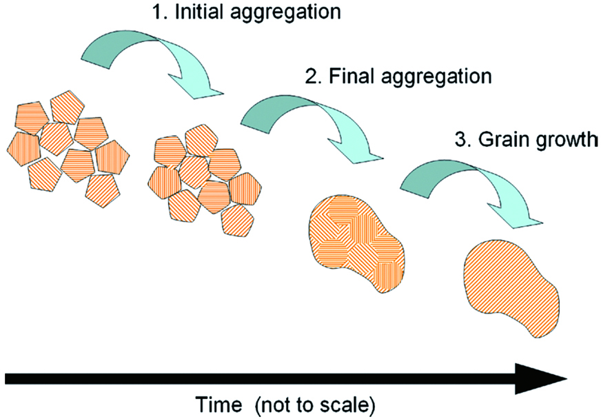
![Schematic showing the mechanisms of coalescence for Au nanoparticles[29]](/richHtml/zgjg/2021/48/8/0802002/img_1.jpg)
Fig. 1. Schematic showing the mechanisms of coalescence for Au nanoparticles[29]
![Coalescence of two Au nanoparticles[30]. (a) TEM images of two Au nanoparticles during the fusion process,the insets are FFT images of selected areas; (b) final structure (136.1 s) of the coalesced Au nanoparticles with its FFT image; (c) coalescence schematic of the (111) twin plane](/richHtml/zgjg/2021/48/8/0802002/img_2.jpg)
Fig. 2. Coalescence of two Au nanoparticles[30]. (a) TEM images of two Au nanoparticles during the fusion process,the insets are FFT images of selected areas; (b) final structure (136.1 s) of the coalesced Au nanoparticles with its FFT image; (c) coalescence schematic of the (111) twin plane
Fig. 3. Die attachment sintered at 300 ℃ using nano-Ag paste[34]. (a) Overview; (b) the enlarged view of region B; (c) the SiC chip/bondline interface; (d) the bondline/DBC substrate interface
Fig. 4. PLD prepared nanostructured films and used as bonding materials[36]. (a) Cooperative mechanism of the CBLDN;(b) paper-based LED using the CBLDN; (c) shear strength of joints; (d) SiC power module using the CBLDN
Fig. 5. The sintering process of Ag nanoparticles[38]. (a) Sintering process started with the nucleation and growth; (b) reduction of Ag cations caused by electron beam irradiation; (c) the aggregation processes of free Ag nanoparticles
Fig. 6. Equilibrium states of Ag nanoparticles and Cu nanoparticles when heated to different temperatures[45]
Fig. 7. Head-to-head welding process of two Au nanorods[49]
Fig. 8. An Ag nanowire junction by laser irradiation[58]. (a) Ag nanowire junctions after irradiation; (b) lattice-resolved TEM image of the interface
Fig. 9. Interconnection between two gold nanocrystals in solution[62]. (a) Bonding between two Au nanocrystals (P and Q) in solution; (b) two Au nanocrystals with common (111) lattice planes yields a nanocrystal with defect at the bonding interface
Fig. 10. Nanowires fabricated via interconnection. (a) Pt nanowires, the insets are high resolution TEM images; (b) Pt3Fe nanorods [64]
Fig. 11. The early growing stages of particles and the corresponding schematic illustrations of particle shapes[65]. (a) A primary particle; (b) lattice matched attachment; (c) twinning attachment growths; (d)--(i) three particles connected through lattice matched attachment or twinning attachment growth
Fig. 12. Interconnection of heterogeneous metallic particles via femtosecond laser irradiation[72]. (a) Nano brazed joint by femtosecond laser irradiation; (b) diagram of bonding interface; (c) interface orientation relationship between Ag-Pt and Ag
Fig. 13. Interconnection of Al and Fe nanoparticles[74]. (a) Morphology of joined Al-Fe nanoparticles by femtosecond laser radiation, the squares represent the corresponding areas; (b)--(d) high resolution TEM images of the areas of b, c, and d
Fig. 14. Interconnection of Ag and Ni nanoparticles[75]. (a) Morphology of joined Ag and Ni nanoparticles, the squares represent the corresponding areas; (b)--(d) high resolution TEM images of the areas of b, c, and d
Fig. 15. Schematic of the welding process of Au-Ag nanoparticles[76]
Fig. 16. TEM images showing the merging of Ag nanoparticles with the Au nanorods[77]
Fig. 17. Fracture process of Au-Ag nanowires after interconnection[78]. (a) Structure of the new Ag-Au nanowire after interconnection; (b) breaking process; (c) breaking position
Fig. 18. The welding of an Au to a Si nanowire using high-intensity electron beam. (a) The original single-crystalline of Au and Si nanowires; (b) joint after exposure for 13 min; (c) the welded region
Fig. 19. Heterogeneous nanowire interconnection[83]. (a) A functional solder joint between nanowires, the I-V curve attached shows the Ohmic behavior of the solder joint; (b) open circuit between nanowires after applying a high current

Set citation alerts for the article
Please enter your email address


