• Photonics Research
  • Vol. 12, Issue 1, 85 (2024)
Andrea Zazzi1, Arka Dipta Das1, Lukas Hüssen2, Renato Negra2, and Jeremy Witzens1、*
Author Affiliations
  • 1Institute of Integrated Photonics, RWTH Aachen University, 52074 Aachen, Germany
  • 2Chair of High-Frequency Electronics, RWTH Aachen University, 52074 Aachen, Germany
  • show less
    DOI: 10.1364/PRJ.493888 Cite this Article Set citation alerts
    Andrea Zazzi, Arka Dipta Das, Lukas Hüssen, Renato Negra, Jeremy Witzens. Scalable orthogonal delay-division multiplexed OEO artificial neural network trained for TI-ADC equalization[J]. Photonics Research, 2024, 12(1): 85 Copy Citation Text show less
    Orthogonal delay-division multiplexing scheme represented for N=3. (a) Power-budget-optimized network architecture, with pilot tone distributed to the downstream layer with separate waveguides. Red and black arrows represent the pilot tone and signals, respectively. (b) Fabrication-tolerant architecture in which the pilot tone and signals are guided together. A time-domain representation of a pulse-based network is also shown.
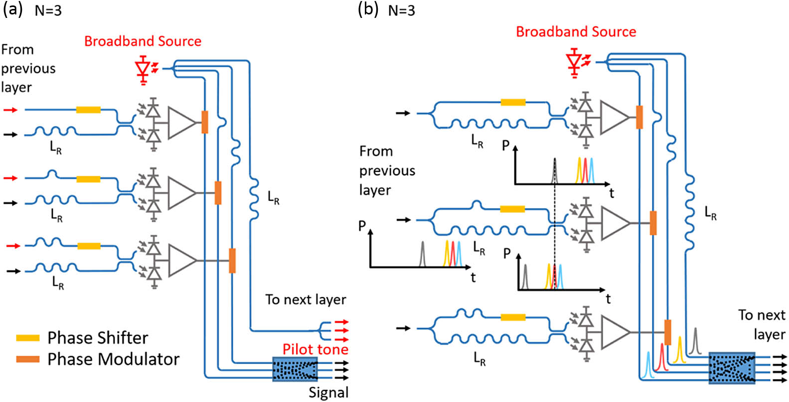
    Fig. 1. Orthogonal delay-division multiplexing scheme represented for N=3. (a) Power-budget-optimized network architecture, with pilot tone distributed to the downstream layer with separate waveguides. Red and black arrows represent the pilot tone and signals, respectively. (b) Fabrication-tolerant architecture in which the pilot tone and signals are guided together. A time-domain representation of a pulse-based network is also shown.
    Signal weighting schemes. In (a), phases can be set independently in the top demodulator branch at the expense of reducing the amplitude proportionally to the number of paths. In (b), this is alleviated by introducing arrayed waveguide gratings to (de-)multiplex the comb lines, allowing, in principle, lossless signal recombination. However, AWGs require a substantial chip area. Significant reduction of the demodulator size is achieved by simultaneously allowing the pilot tone to cross each path in the upper demodulator branch of (c) so that a programmable superposition of all possible combinations of delays is obtained. (d) Further simplified network in which the embedded MZIs have been replaced by static splitters with an off-3-dB splitting ratio.
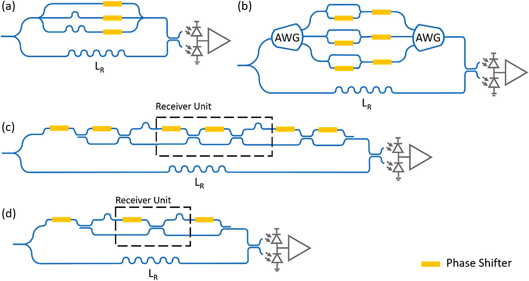
    Fig. 2. Signal weighting schemes. In (a), phases can be set independently in the top demodulator branch at the expense of reducing the amplitude proportionally to the number of paths. In (b), this is alleviated by introducing arrayed waveguide gratings to (de-)multiplex the comb lines, allowing, in principle, lossless signal recombination. However, AWGs require a substantial chip area. Significant reduction of the demodulator size is achieved by simultaneously allowing the pilot tone to cross each path in the upper demodulator branch of (c) so that a programmable superposition of all possible combinations of delays is obtained. (d) Further simplified network in which the embedded MZIs have been replaced by static splitters with an off-3-dB splitting ratio.
    Numerical trials for the validation of the weight space addressable by the demodulator architecture shown in Fig. 2(c). Trials are categorized as having failed when a suitable PS-configuration cannot be found to reach the randomly generated set of target weights. For each data point, corresponding to a given weight scenario and scaling parameter μ, 1000 random trials are run, and the failures with actual-to-target deviations above 1% and 10% are counted.
    Fig. 3. Numerical trials for the validation of the weight space addressable by the demodulator architecture shown in Fig. 2(c). Trials are categorized as having failed when a suitable PS-configuration cannot be found to reach the randomly generated set of target weights. For each data point, corresponding to a given weight scenario and scaling parameter μ, 1000 random trials are run, and the failures with actual-to-target deviations above 1% and 10% are counted.
    Diagram of a 31×31 network. Devices defined in the SiN and Si layers are shown in green and blue, respectively. Delay loops required to shift signals and pilot tone between ODDM channels are shown explicitly in the Tx network and in the inset showing the demodulator, with each circle symbolizing a loop of length L0.
    Fig. 4. Diagram of a 31×31 network. Devices defined in the SiN and Si layers are shown in green and blue, respectively. Delay loops required to shift signals and pilot tone between ODDM channels are shown explicitly in the Tx network and in the inset showing the demodulator, with each circle symbolizing a loop of length L0.
    Exemplary simulation result with a comb FWHM spanning 75% of Δν and a Bessel filter cutoff frequency of 6.25 GHz. (a) Normalized demodulated photocurrent versus transmitted signal for each of the 31 channels and (b) difference between the transmitted and the normalized received signals. Its std. dev. is σδ=0.073.
    Fig. 5. Exemplary simulation result with a comb FWHM spanning 75% of Δν and a Bessel filter cutoff frequency of 6.25 GHz. (a) Normalized demodulated photocurrent versus transmitted signal for each of the 31 channels and (b) difference between the transmitted and the normalized received signals. Its std. dev. is σδ=0.073.
    Signal distortion (std. dev. of the difference between the demodulated photocurrent and the transmitted signal) versus (a) comb FWHM and (b) Bessel filter cutoff frequency. In (a), the Bessel filter cutoff is maintained at 6.25 GHz, and in (b), the FWHM is maintained at 1.5Δν (75 nm). The inset of panel (a) displays the comb spectrum normalized to a peak comb line power of 1, and the inset of panel (b) shows the transfer function of the assumed Bessel filter.
    Fig. 6. Signal distortion (std. dev. of the difference between the demodulated photocurrent and the transmitted signal) versus (a) comb FWHM and (b) Bessel filter cutoff frequency. In (a), the Bessel filter cutoff is maintained at 6.25 GHz, and in (b), the FWHM is maintained at 1.5Δν (75 nm). The inset of panel (a) displays the comb spectrum normalized to a peak comb line power of 1, and the inset of panel (b) shows the transfer function of the assumed Bessel filter.
    Simulated noise std. dev. σδ versus (a) assumed optical and RF comb source linewidths and (b) optical comb source power. In both (a) and (b), the comb FWHM is set to 1.5Δν. In (a), the Bessel filter cutoff is set to 6.25 GHz, and shot noise and thermal noise are ignored to maintain a low noise floor, allowing us to estimate the impact of the linewidths on their own. In (b), these noise sources are turned on. Moreover, the target scenario with a 12.5 GHz Bessel cutoff frequency is assumed to obtain the corresponding NEB. This includes the higher distortion floor established in Subsection 4.A. Arrows in (a) and (b) indicate the operating conditions assumed in the following.
    Fig. 7. Simulated noise std. dev. σδ versus (a) assumed optical and RF comb source linewidths and (b) optical comb source power. In both (a) and (b), the comb FWHM is set to 1.5Δν. In (a), the Bessel filter cutoff is set to 6.25 GHz, and shot noise and thermal noise are ignored to maintain a low noise floor, allowing us to estimate the impact of the linewidths on their own. In (b), these noise sources are turned on. Moreover, the target scenario with a 12.5 GHz Bessel cutoff frequency is assumed to obtain the corresponding NEB. This includes the higher distortion floor established in Subsection 4.A. Arrows in (a) and (b) indicate the operating conditions assumed in the following.
    (a) Simulated noise std. dev. σδ versus group delay mismatch applied in the Tx branches. The Bessel filter cutoff is set to 6.25 GHz, and the noise sources are turned off to obtain a low noise floor allowing us to estimate the impact of the group delay mismatch alone. (b) Histogram of the demodulated signal error with the Bessel filter cutoff set to the nominal 12.5 GHz, noise sources turned on, and device non-idealities considered.
    Fig. 8. (a) Simulated noise std. dev. σδ versus group delay mismatch applied in the Tx branches. The Bessel filter cutoff is set to 6.25 GHz, and the noise sources are turned off to obtain a low noise floor allowing us to estimate the impact of the group delay mismatch alone. (b) Histogram of the demodulated signal error with the Bessel filter cutoff set to the nominal 12.5 GHz, noise sources turned on, and device non-idealities considered.
    (a) Schematic of the auxiliary SiN chip generating the 25 GHz comb shared between the OE-TI-ADC front-end and the OEO-ANN. Prior to routing it to the ANN, the FSR of the comb is doubled with an imbalanced MZI. (b) Six-channel OE-TI-ADC front-end. Interleaved pulse trains with different center frequencies are fed to a dual-output MZM, after which the pulse trains are de-interleaved by a wavelength division demultiplexer. (c), (d) Schematics of the ANN input layer. In (c), required delays are implemented in the electrical domain, prior to electro-optic phase modulation. In (d), signals are split and delayed in the optical domain instead, with delays chosen such that the delayed optical signals are mapped to free ODDM channels. (e) Higher-level schematic of the overall ANN, with two optical networks connecting, respectively, the input to the hidden layer (11×31) and the hidden layer to the output layer (31×31), whose output can be directly decoded with binary electronics.
    Fig. 9. (a) Schematic of the auxiliary SiN chip generating the 25 GHz comb shared between the OE-TI-ADC front-end and the OEO-ANN. Prior to routing it to the ANN, the FSR of the comb is doubled with an imbalanced MZI. (b) Six-channel OE-TI-ADC front-end. Interleaved pulse trains with different center frequencies are fed to a dual-output MZM, after which the pulse trains are de-interleaved by a wavelength division demultiplexer. (c), (d) Schematics of the ANN input layer. In (c), required delays are implemented in the electrical domain, prior to electro-optic phase modulation. In (d), signals are split and delayed in the optical domain instead, with delays chosen such that the delayed optical signals are mapped to free ODDM channels. (e) Higher-level schematic of the overall ANN, with two optical networks connecting, respectively, the input to the hidden layer (11×31) and the hidden layer to the output layer (31×31), whose output can be directly decoded with binary electronics.
    (a) Photocurrent at the output of the analog output ANN as a function of its input (bottom axis). The nonlinearity of the system is apparent. The ANN corrects for the OE-TI-ADC front-end nonlinearity, as shown by the red curve. It corresponds to the output of the ANN as a function of the input to the OE-TI-ADC (top axis) and has a very linear profile. In (b), the photocurrent of every third output neuron of the digital output ANN is shown as a function of the input to the ANN. The crossing of these curves with the zero differential photocurrent level corresponds to the switching threshold of the following 1-bit digitizer.
    Fig. 10. (a) Photocurrent at the output of the analog output ANN as a function of its input (bottom axis). The nonlinearity of the system is apparent. The ANN corrects for the OE-TI-ADC front-end nonlinearity, as shown by the red curve. It corresponds to the output of the ANN as a function of the input to the OE-TI-ADC (top axis) and has a very linear profile. In (b), the photocurrent of every third output neuron of the digital output ANN is shown as a function of the input to the ANN. The crossing of these curves with the zero differential photocurrent level corresponds to the switching threshold of the following 1-bit digitizer.
    (a) SNR levels of the processed signals in different scenarios, highlighting the improvement with respect to the non-equalized signal, also in presence of noise. The SNR is assessed by processing sinusoidal signals at the frequencies reported on the abscissa. In (b), the mean SNR, assessed by averaging the variances of signals at multiple frequencies, is shown as a function of different rescaling factors applied to the std. dev. of the noise terms. The analog output ANN is seen to be significantly more sensitive to noise than the digital output ANN.
    Fig. 11. (a) SNR levels of the processed signals in different scenarios, highlighting the improvement with respect to the non-equalized signal, also in presence of noise. The SNR is assessed by processing sinusoidal signals at the frequencies reported on the abscissa. In (b), the mean SNR, assessed by averaging the variances of signals at multiple frequencies, is shown as a function of different rescaling factors applied to the std. dev. of the noise terms. The analog output ANN is seen to be significantly more sensitive to noise than the digital output ANN.
    DCS design and characteristics. (a) Layout of the DCS designed into the 220 nm SOI device layer, (b) power transmission coefficients, and (c) group delays associated with the four port combinations labeled in (a) after balancing with external waveguide segments sized for 1550 nm.
    Fig. 12. DCS design and characteristics. (a) Layout of the DCS designed into the 220 nm SOI device layer, (b) power transmission coefficients, and (c) group delays associated with the four port combinations labeled in (a) after balancing with external waveguide segments sized for 1550 nm.
    Star coupler design and characteristics. (a) Layout of the star coupler with overlaid field intensity for light injected through the port of index −15.5. (b) Power transfer coefficients and (c) group delays for light injected through one of the two centermost waveguides (black) and light injected through the waveguide of index l=−15.5 (red markers).
    Fig. 13. Star coupler design and characteristics. (a) Layout of the star coupler with overlaid field intensity for light injected through the port of index 15.5. (b) Power transfer coefficients and (c) group delays for light injected through one of the two centermost waveguides (black) and light injected through the waveguide of index l=15.5 (red markers).
    Floorplan of a 31-by-31 ANN-PIC. The insets show details of the layout.
    Fig. 14. Floorplan of a 31-by-31 ANN-PIC. The insets show details of the layout.
    Andrea Zazzi, Arka Dipta Das, Lukas Hüssen, Renato Negra, Jeremy Witzens. Scalable orthogonal delay-division multiplexed OEO artificial neural network trained for TI-ADC equalization[J]. Photonics Research, 2024, 12(1): 85
    Download Citation