We demonstrate a large-mode-volume transverse-electric-polarized shifted distributed feedback (DFB) cavity on silicon-on-insulator (SOI). A 2.86 mm-long DFB cavity with sidewall corrugation on the ridge is fabricated on a silicon rib waveguide. The cavity structure is designed to enlarge both the longitudinal and transversal mode profiles of the cavity to enclose more luminescent media. Design strategies are verified by both finite difference time domain simulation and experiments. A linewidth of 69 pm and an extinction ratio of 15 dB is obtained, indicating not only the well confinement of the longitudinal mode, but also its well stretching to the cavity ends. The mode volume is .
Distributed feedback (DFB) structures have found numerous applications in the field of optoelectronics, ranging from semiconductor lasers to optical filters[1,2]. Since the 1970s, optical properties of different kinds of DFB structures[3,4] on III-V material platforms and erbium-doped fibers[5] have been fully explored to improve laser properties such as threshold, linewidth, and stability. Utilization of DFB structures on silicon-on-insulator (SOI) platforms has been an emerging trend in recent decades[6–8]. Because of their free spectral range (FSR)-free, high design flexibility, and comparatively easy fabrication process, DFB structures have been widely used in applications like on-chip optical filters, contra-directional couplers[9], and dispersion engineering[10]. However, these applications are mostly restricted to passive devices. For realizing on-chip optical interconnection, one of the essential components is the on-chip light source, which is usually composed of a luminescent medium and a single-resonance cavity. Various kinds of silicon-based luminescent media have been intensively studied in recent years[11,12]. Silicon-based light-emitting devices based on Ge quantum dots in optical microcavities are reported in recent years, showing a possible candidate for silicon-based light sources[13,14]. However, these Ge quantum dots-based microcavities are multimode in operation and had a mode volume less than several cubic micrometers, resulting in a low optical emitted power of several picowatts[15] and preventing them from optical source application in on-chip optical interconnection.
A single-resonance cavity with a large mode volume is required to increase the output power of a Ge dots-based light-emitting device. Compared to a microring and a photonic crystal microcavity, the DFB cavity provides resonance at a single wavelength rather than multiple wavelengths and has a much larger mode volume. These advantages make it a good candidate for on-chip light-emitting devices. In this letter, we optimize both the longitudinal and transverse mode profiles of a shifted DFB cavity on a SOI platform to obtain a larger mode volume of the resonant mode compared with microring and photonic crystal microcavities. The relationship between the mode profile, resonance linewidth, and DFB structure parameters is numerically investigated. There is a tradeoff between the narrow linewidth and the flatness of the longitudinal mode distribution. A large-mode-volume DFB cavity with a resonance linewidth of 69 pm is experimentally demonstrated by addressing the tradeoff.
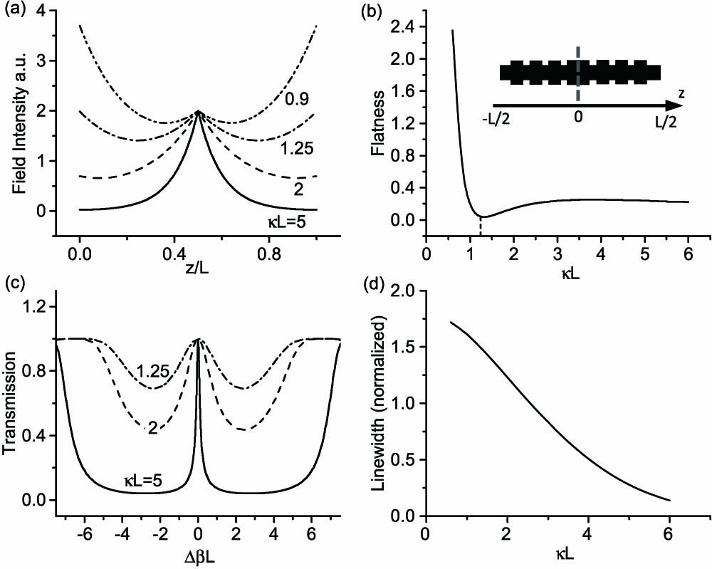
The longitudinal mode distribution of a phase-shifted DFB cavity can be calculated by solving a multisection boundary value problem using coupled mode equations[16]. The transmission spectrum can be calculated using a fundamental matrix ( matrix) approach that is also based on coupled mode theory (CMT)[17]. Both methods divide the cavity into two uniform grating segments that have a phase difference. The DFB cavity is illustrated schematically by the inset in Fig. 1(b), which is the top view of a sidewall-modulated waveguide. Light propagates in a waveguide along the direction. is the cavity length and is the coupling coefficient. is the normalized coupling coefficient, which represents total coupling capacity of the cavity.
Sign up for Chinese Optics Letters TOC. Get the latest issue of Chinese Optics Letters delivered right to you!Sign up now
Figure 1.(a) Longitude mode distribution and (c) the transmission spectrum of a shifted DFB cavity for different values of , (b) flatness of the longitude mode profile versus , and (d) the linewidth of the resonance mode versus .
Figure 1(a) shows the calculated longitudinal mode at different . As decreases, a less portion of light tends to concentrate on the central phase-shifted region and the mode become more flat. When reduces to less than 1.25, the mode spreads toward both ends of the cavity, resulting in deterioration of flatness. The degree of flatness of the intensity distribution for the DFB mode is defined as[18]where is the average light intensity inside the cavity. Smaller represents better flatness. Since more luminescent media can participate in light emission when the mode profile is flat, it is necessary to find the optimal to obtain the minimal F. Figure 1(b) shows the mode flatness as a function of . As shown by the curve, a minimum flatness appears at , which is the optimal value without considering the linewidth of resonance. However, as shown by the transmission spectra in Fig. 1(c), the linewidth of the resonance is much wider at than at . is the normalized (by cavity length) propagation constant difference from the Bragg condition (i.e., the resonant wavelength). The relationship between the linewidth and is shown in Fig. 1(d), where the linewidth decreases monotonically as increases. Therefore, there is a tradeoff between longitudinal flatness and the narrow linewidth of the resonant mode. A larger means larger feedback along the grating and more light is concentrated in the cavity center while less is coupled out at the cavity ends, as shown in Fig. 1(a). This results in a higher factor and then a smaller linewidth. To enlarge the absolute size of the longitudinal mode, we increase to stretch the absolute size of the longitudinal mode while keeping constant. The normalized longitudinal mode profile does not change since it is determined by . The absolute resonance linewidth will decrease by increasing as is kept constant due to unchanged .
To illustrate the stretching of the absolute size of the longitudinal mode, a finite difference time domain (FDTD) simulation of the shifted DFB cavity is performed. Three DFB cavities with the same of 3 and different lengths of , 50, and 75 μm are simulated. The simulation results are shown in Fig. 2. All three cavities have the same longitude mode distribution after being normalized by the cavity length. As shown by the comparison of three cavities, the absolute mode size of the longest cavity is larger than that of the others, i.e., the absolute size of the longitudinal mode is stretched due to the long cavity length.
Figure 2.2D-FDTD simulation result of shifted DFB cavity: the mode profile of the three cavities with lengths of 25, 50, and 75 μm.
To increase while keeping constant, a smaller coupling coefficient is required. Grating feedback can be introduced by corrugating the sidewall of the waveguide on a SOI wafer. The realization of a small and precise controllable coupling coefficient is discussed in the strip and rib waveguide below.
A 2D finite element algorithm is used to solve the mode profile and effective index of the fundamental transverse-electric (TE) mode in both the strip and rib waveguide on a SOI wafer with 220 nm-thick top silicon. Figure 3(a) shows a comparison of the coupling coefficient of the rib waveguide and strip waveguide at different corrugation lengths. Figures 3(b) and 3(c) show the corrugation length (indicated by the dashed line) and the mode profile of fundamental TE mode for the rib and strip waveguide, respectively. The width of both waveguides are 650 nm. The ridge height of the rib waveguide is 80 nm. The coupling coefficient is calculated by [19], where and are the effective indices of the fundamental mode with and without sidewall corrugation. is the Bragg wavelength of the grating and is 1,550 nm here. As shown in Fig. 3(a), the coupling coefficient monotonically increases with the corrugation length d. For a constant corrugation length, the rib waveguide has a much smaller coupling coefficient than the strip waveguide. The curve slope of the rib waveguide is more gradual than that of the strip waveguide, indicating that more precise controllability of the coupling coefficient can be realized in the rib waveguide. Moreover, the 650 nm wide strip waveguide is multimode and a narrower width is required to achieve single-mode operation, which will further increase its lowest achievable coupling efficiency.
Figure 3.(a) Coupling coefficient of the rib and strip waveguide as a function of the corrugation length and field distribution of the fundamental TE mode for (b) the rib and (c) the strip waveguide, where the dashed line indicates the sidewall corrugation.
These advantages of a rib waveguide can be explained by the overlap between the optical mode field and the sidewall corrugation. As shown in Fig. 3(c), the optical field in the strip waveguide has a considerable overlap with the sidewall. Because of the high index contrast of the SOI platform, the coupling coefficient of the sidewall-corrugated strip waveguide is strong even with small corrugation length, whereas in the rib waveguide, the overlap is only on the ridge and is smaller than that of the strip waveguide. Smaller overlap introduces a weaker coupling coefficient. Considering the resolution limits of the electron beam lithography system, it is easier to achieve a small and more controllable coupling coefficient by corrugating the sidewall of the rib waveguide. The mode profile of the rib waveguide is larger than for the strip waveguide, implying more luminescent media can be enclosed and participate in light emission. To achieve a small and precise controllable coupling coefficient, the rib waveguide with sidewall corrugation on its ridge is applied in our Bragg grating of the DFB cavity.
To validate the design strategy, shifted DFB cavities are fabricated on a silicon rib waveguide with 650 nm ridge width and 80 nm etched depth. Sidewall corrugation is on both sides of the rib waveguide. Grating pitch and duty factor are adjusted to be 288 nm and 50% to align the resonance peak around 1550 nm. Three examples of cavity geometries are chosen, i.e., cavity A with 25 nm corrugation length, 1760 periods; cavity B with 25 nm corrugation length, 3800 periods, and cavity C with 9 nm corrugation length, 10000 periods. Cavities A and B have the same coupling coefficient due to the same corrugation length. Cavities B and C have similar but different coupling coefficients and cavity lengths. All cavities are fabricated on a SOI wafer with 220 nm thick top silicon and 3000 nm thick silica. Electron beam lithography (EBL, Vistec EBPG 5000 Plus) and inductively coupled plasma (ICP) etch are used to define the DFB cavities’ patterns. Both ends of the cavities are terminated by integrated grating couplers designed for TE polarization, which couples light between a silicon waveguide and a SMF-28 single-mode fiber tilted at 10° to the normal direction of the SOI slab. Figure 4 shows a scanning electron microscope (SEM) micrograph of the phase-shifted region of the DFB cavity and an optical microscope micrograph of the whole cavity for cavity C. The measured width of the waveguide is 4 nm narrower than the designed value because of side etching during the ICP process. The sidewall corrugation is shown in the inset of Fig. 4(a). Due to the short corrugation length (9 nm) used to achieve a small coupling efficient, this kind of sidewall corrugated DFB cavity can only be fabricated by EBL equipment. A small coupling coefficient can also be achieved by placing pillars around the waveguide[7], in which case the dimension is large enough to be fabricated in a CMOS compatible environment using deep-UV (DUV) lithography.
Figure 4.(a) SEM image of the phase-shift region and the sidewall corrugation (inset) of the DFB cavity and (b) optical microscope micrographs of the whole cavity C.
The transmission spectrum of each cavity is obtained by coupling light from an amplified spontaneous emission (ASE) light source into the cavity through the fiber-to-waveguide grating coupler. A grating coupler on the other side of the cavity couples the output light into an optical spectrum analyzer (OSA, YOKOGAWA AQ6370B), as shown in Fig. 5(a). The measured transmission spectra for cavities A, B, and C are shown in Fig. 5(b). The resonance peak of each cavity is located inside the stop band of the DFB grating. The inset in Fig. 5(b) shows the Lorentz fit of the resonance peak for cavity C. The deviation of the resonance peak from the stop band center may be attributed to the write-field stitching error of the EBL system. These three kinds of cavities were etched separately with the same etching parameters, by the same ICP equipment. The variation of etching depth results in the measured resonant wavelength shift between each cavity. The observation of resonance around the designed wavelength indicates the fundamental-mode operation of the rib waveguide.
Figure 5.(a) Illustration of the measurement experiment setup and (b) the measured transmission spectrum of cavities A, B, and C. The inset is a Lorentz fit of the resonance peak for cavity C.
For spectrum analysis, the coupling coefficient is calculated from the spectrum by fitting the stop band width with CMT[20]. The linewidth of the resonance is obtained from Lorentz fitting. The coupling coefficient (), cavity length, , and resonance linewidth of each cavity are shown in Table 1.
Due to the larger and longer cavity length of cavity B, cavity B has a smaller linewidth than cavity A. Cavities B and C have a similar , while the resonance linewidth of cavity C is half the linewidth of cavity B owing to a smaller coupling coefficient and a longer longitudinal mode. These experimental results are consistent with the numerical analysis and simulation results discussed above. With the same , the resonance peak of cavity C shows more coupling loss than cavity B, which is due to a larger propagating loss in a longer cavity. The resonance peak of cavity C has an extinction ratio of 15 dB, indicating a well stretching of the longitudinal mode to both ends of the 2.86 mm-long cavity. We use the conventional definition of the cavity mode volume, which is the ratio of the total electric field energy to the maximum of the electric field energy density. Using the fitted coupling coefficient, the mode volume of cavity C is calculated to be , which is 1000 times larger than the photonic crystal L3 cavity[21].
The key point of DFB cavity fabrication is precise controllability of the coupling coefficient, since it directly affects cavity length, stop band width, and resonance linewidth. The realization of well controllable coupling coefficient may favor various applications. For example, a small coupling coefficient with long cavity may be used for on-chip light emitting cavities as discussed by this Letter. A large coupling coefficient with a small cavity size may be used for compact add-drop filtering applications, as its wide stop band could block unwanted frequencies while letting the wanted frequency pass through the resonance peak whose linewidth can be controlled by varying . To experimentally examine the controllability of the coupling coefficient, a series of shifted DFB cavities based on an 80-nm etched rib waveguide with a different corrugation length were fabricated on the same wafer. All coupling coefficients are measured by the same approach mentioned above. It should be noted that the CMT assumptions break down for very large values of corrugation length and consequently the results become less accurate in that case. The results are shown in Fig. 6. The coupling coefficient shows an approximately linear relation with the corrugation length in the weak coupling region. The linearly fitted slope coefficient is 1.442 and the measured coupling coefficients show a small deviation from the fitted line, suggesting a good fabrication controllability and tolerance of the coupling coefficients.
Figure 6.Coupling coefficient as a function of the corrugation length on the rib waveguides.
In conclusion, we demonstrate a shifted DFB cavity with a large longitudinal resonant mode using a shallow etched rib waveguide on a SOI wafer. We numerically and experimentally show that the longitudinal mode profile can be stretched by keeping the normalized coupling coefficient constant and decreasing the coupling coefficient. The coupling coefficient can be controlled by the sidewall corrugation length on the ridge. A DFB cavity with 9 nm corrugation length, 2.86 mm cavity length, 69 pm linewidth, and an extinction ratio of 15 dB are demonstrated. The mode volume is , which is three orders of magnitude larger than for a typical photonic crystal cavity. The large-mode-volume DFB cavity demonstrated here can enclose more luminescent media and has the potential to increase the output power of silicon-based light emitters based on Ge quantum dots embedded in cavities. Moreover, assisted by a good controllability of the coupling coefficient, this design strategy of the DFB cavity can also be used in various applications, such as optical switching and add-drop filtering.