1Center for Optics Research and Engineering, Key Laboratory of Laser & Infrared System, Ministry of Education, Shandong University, Qingdao 266237, China
2School of Information Science and Engineering, Shandong University, Qingdao 266237, China
【AIGC One Sentence Reading】:This study introduces an electrically tunable PCM-based metasurface for dynamic infrared thermal camouflage, addressing challenges like temperature uniformity and amorphization, paving the way for advanced thermal concealment in varying environments.
【AIGC Short Abstract】:This study introduces an electrically tunable phase-change metasurface for dynamic infrared thermal camouflage. By harnessing phase change materials, the design offers wide emissivity tuning, rapid modulation, and adaptability to various backgrounds. Simulation results showcase its spectral tuning range, quench rates for amorphization, and camouflage capabilities, marking a significant step forward in practical thermal camouflage technology with potential civil and military applications.
Note: This section is automatically generated by AI . The website and platform operators shall not be liable for any commercial or legal consequences arising from your use of AI generated content on this website. Please be aware of this.
Abstract
Dynamic infrared thermal camouflage technology has attracted extensive attention due to its ability to thermally conceal targets in various environmental backgrounds by tuning thermal emission. The use of phase change materials (PCMs) offers numerous advantages, including zero static power, rapid modulation rate, and large emissivity tuning range. However, existing PCM solutions still encounter several practical application challenges, such as temperature uniformity, amorphization achievement, and adaptability to different environments. In this paper, we present the design of an electrically controlled metal-insulator-metal thermal emitter based on a PCM metasurface, and numerically investigate its emissivity tunability, physical mechanisms, heat conduction, and thermal camouflage performance across different backgrounds. Furthermore, the influence of the quench rate on amorphization was studied to provide a guidance for evaluating and optimizing device structures. Simulation results reveal that the thermal emitter exhibits a wide spectral emissivity tuning range between 8 and 14 μm, considerable quench rates for achieving amorphization, and the ability to provide thermal camouflage across a wide background temperature range. Therefore, it is anticipated that this contribution will promote the development of PCM-based thermal emitters for practical dynamic infrared thermal camouflage technology with broad applications in both civilian and military domains.
1. INTRODUCTION
The ability to control infrared thermal radiation plays a pivotal role in extensive application fields, including thermal camouflage [1–3], infrared detection [4,5], thermophotovoltaics [6–8], radiative cooling [9–11], and thermal management [12,13]. In particular, there is growing interest in the field of infrared thermal camouflage due to its capability to shield targets from detection by matching their thermal radiation with that of the surrounding environment. Infrared thermal camouflage is typically achieved by altering the emissivity of an object, offering high flexibility, robust controllability, and fast manipulation. Traditional methods of achieving infrared thermal camouflage technologies such as infrared camouflage coating, nets, and masks, as well as more recent developments like silicon nanowires/silver nanoparticles flexible films [14], Ag/Ge multilayer films [15], hierarchical metamaterials [16], and MXene films [17], are constrained by their fixed emissivity. Consequently, these approaches are limited to specific background temperature ranges, rendering them ineffective when the target’s location or the background temperature changes. Therefore, it is urgent to develop dynamic infrared thermal camouflage technology that adapts to diverse environmental backgrounds.
Recently, some regulatory mechanisms for dynamic infrared thermal camouflage have been reported, including the dynamic control of intersubband absorption in n-type quantum wells [18], the reversible intercalation of nonvolatile ionic liquids into multilayer graphene [19], the reversible wetting modulation of porous polymer coatings [20], and so on. However, these methods still face several challenges in practical applications: 1) the requirement of continuous external electric power to maintain the required emissivity of the target due to their volatile nature, resulting in high power consumption [18,19]; 2) narrow tuning range of emissivity, limiting adaptability to various environments [21]; and 3) slow modulation speed, restricting the potential applications under conditions of rapid background temperature change [20,22]. To overcome these problems, nonvolatile metal-insulator-metal (MIM) structures based on chalcogenide phase-change materials (PCMs) have been proposed in recent years [23–25], which exhibit distinct advantages with zero-static power consumption, fast modulation rate, and large tunable range. This is thanks to the fact that PCMs possess nonvolatile stable amorphous and crystalline phases at room temperature [26], which have notable distinctions in aspects of complex refractive index and resistivity and can be switched in nanoseconds and even sub-nanoseconds by means of thermal, electric, and optical stimulations [27].
So far, there have been two main categories of dynamic infrared thermal camouflage devices based on PCMs: multilayer film type and metasurface type. The multilayer film type devices control their spectral emissivity by regulating interlayer interference and generally possess a wide incident angle range, polarization insensitivity, and omni-direction. Besides, they can be easily fabricated by mature coating methods, for example, magnetron sputtering. In 2018, Qu et al. demonstrated that a (GST)-Au bilayer film could realize stealthiness in thermal camera images under different background temperatures by changing the annealing time [25]. In 2022, Quan et al. proposed some Mo-GST stack structures and numerically proved that they could be switched between infrared ‘stealthy’ and ‘non-stealthy’ states [28]. Kim et al. utilized a laser printing method to customize thermal emission by spatially tuning the phase of GST in the longitudinal direction [29]. The metasurface type, based on the MIM plasmonic resonance effect, achieves thermal camouflage by optimizing the geometry parameters of devices and stimulating the phase transition of the PCMs. Most of the time, metasurface devices are fabricated by photolithography. Compared to the former, the metasurface type devices usually exhibit polarization sensitivity if non-cylindrical symmetry exists in geometric structures and has a narrower permissible range of incident angles but offers more design freedom and needs more sophisticated lithography process. Qu et al. experimentally demonstrated the dynamic tuning of thermal emission of a GST-based thermal emitter by exciting different magnetic resonance modes [30,31]. Kang et al. conducted a detailed numerical investigation of this kind of thermal emitter, examining aspects such as physical mechanism, emissivity tunability, incident angles, polarization dependence, and the range of background temperatures over which it can provide stealth capability [32].
However, there are still several difficulties hindering the practical applications of the aforementioned solutions. First, these reports did not study device performance in terms of heat conduction, temperature uniformity, and cooling rate, which are necessary for implementing the crystallization and amorphization processes of PCMs. For example, amorphous GST begins to crystallize when temperature rises to approximately 160°C, and crystalline GST transitions to the amorphous phase under the condition of an ultrahigh quench rate () after melting. Second, the use of a thick GST layer () inevitably leads to large internal temperature differences and a slower quench rate. Third, all the experimental articles lack amorphization results, primarily due to improper device design and stimulation methods, such as using a thick GST layer and employing hotplate heating means. These factors render the emissivity switching almost disposable, making the devices unable to accommodate diverse environmental backgrounds.
To address these challenges, this paper introduces an electrically controlled emissivity-tunable GST-based MIM thermal emitter, aimed at achieving practical dynamic infrared thermal camouflage. The MIM thermal emitter consists of a bottom Pt layer, a middle GST layer, and a top Au pillar array, where the Pt layer is used to connect external electric pulses to induce a phase transition of the GST layer by Joule heating. An electromagnetic model, combined with the effective medium theory, is established to numerically simulate the spectral emissivity under different crystallization fractions of GST and unravel the underlying physical mechanism. Our study employs a multi-physics phase transition code to investigate the impact of the quench rate on the amorphization process of GST. Additionally, the heat conduction and temperature distribution are calculated at different electric pulses to assess the quench rate and temperature uniformity within GST. Lastly, we compute the background temperature ranges in which thermal camouflage can be achieved for different real object temperatures and two distinct backgrounds. The numerical results demonstrate that our proposed GST-based MIM thermal emitter can use external electric pulses to induce the phase transition of GST and adjust the spectral emissivity of the device. This approach shows significant potential for practical applications. Hence, we foresee that this thermal emitter will pave the way for high-performance dynamic infrared thermal camouflage with zero-static power consumption and a large adaptive background temperature range.
2. METHODS
A. Structure Design
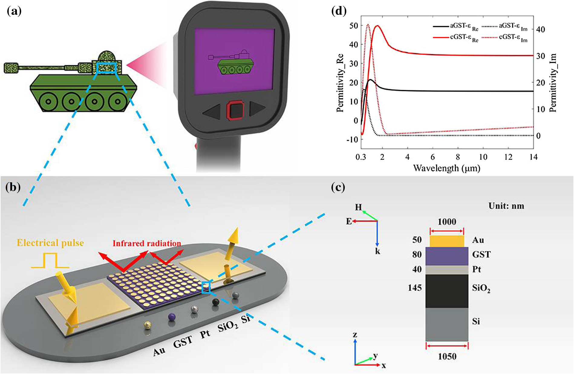
Dynamic thermal camouflage can achieve low observability of a target by effectively modifying the infrared radiation intensity to blend with its surroundings. Figure 1(a) illustrates a schematic where the upper portion of a target, covered by thermal camouflage structures, blends into the background when observed using infrared detection equipment. Figure 1(b) depicts the structural schematic of our proposed dynamic infrared thermal camouflage configuration, and Fig. 1(c) presents a sectional view of a unit cell.
Figure 1.(a) Schematic of an infrared thermal camouflage scenario. (b) Perspective view and (c) cross-sectional view of electrically controlled dynamic infrared thermal camouflage structures based on GST. The metasurface consists of an Au pillar array, a GST layer, a Pt layer, a layer, and a Si substrate. (d) Permittivities of GST across the visible to infrared wavebands.
The configuration belongs to an electrically reconfigurable nonvolatile thermal emitter whose core functional component is an MIM plasmonic metasurface consisting of Pt-GST-Au layers. The 40-nm-thick bottom Pt layer serves a dual purpose, acting as a barrier to prevent transmittance across a broad infrared band and functioning as a Joule heating layer to induce the phase transition of GST. The middle GST layer with a thickness of 80 nm controls the emissivity of the thermal emitter by tuning the peaks of the MIM plasmonic resonance. The top Au layer is designed as a periodic cylindrical array with a height of 50 nm, a diameter of 1000 nm, and a period of 1050 nm. The MIM metasurface is situated on a Si substrate with high thermal conductivity, allowing for rapid dissipation of Joule heat to facilitate the amorphization process. To enhance the electric heating efficiency, a low thermal conductivity layer with a thickness of 145 nm is introduced between the MIM metasurface and the substrate. Two large Au pads are used to guide the electrical pulses into the Pt layer.
B. Optical Simulation
The infrared thermal radiation characteristics of the GST-based thermal emitter were simulated using a finite-difference time-domain model. Due to the periodicity of the metasurface, the model only needs to compute a unit cell by applying the periodic boundary condition to both and in-plane directions. The perfectly matched layer boundary condition was set along the out-of-plane -direction. The absorption spectra were calculated by recording the reflection and transmission spectra with an -plane power monitor. The permittivity versus wavelength [0.3–14 μm, shown in Fig. 1(d)] of GST was obtained from Ref. [33] and those of other materials were obtained from Palik’s handbook. The electric field () and the magnetic field () were along the - and -directions, respectively, while the wave vector () was along the -direction.
C. Thermal Simulation
The electric heating simulations were conducted using a three-dimensional finite-element multi-physics model. The model consisted of an electric current module and a in-solids heat transfer module. In the electric current module, a nanosecond electrical pulse with varying voltage and width was applied between two Au pads. In the heat transfer module, a constant room temperature was used for both the side and bottom boundaries, and a thermally insulated boundary condition was applied on the top surface. To reduce the number of meshes and computation time, the top Au layer was regarded as a homogenous layer where no electric current passed, rather than a cylindrical array. The thermal properties of GST in the model were derived from Ref. [34]. The thermal conductivities of the amorphous GST (aGST) and crystalline GST (cGST) are and , respectively. The heat capacity of GST is .
3. RESULTS AND DISCUSSIONS
A. Emissivity of GST-based MIM Thermal Emitter
GST exhibits strong stability in both its amorphous and crystalline phases at room temperature. Upon heating, aGST undergoes a transformation into cGST at approximately 160°C. When cGST is heated to a temperature above its melting point () and then rapidly cooled to room temperature, it reverts back to the amorphous phase [31,35]. During the phase transition process or under incomplete transition conditions, GST exists in an intermediate stage that consists of a homogeneous mixture of both crystalline and amorphous molecules in varying proportions. For example, as the temperature increases to the crystallization temperature, crystalline nuclei of GST first appear in an amorphous film, subsequently form the intermediate phase, and finally combine to develop the complete crystalline structure. To investigate the emissivity of the MIM thermal emitter at different intermediate phases of GST, the effective permittivity of GST was calculated using the effective medium theory [36] based on the Lorentz–Lorenz relation [37–39], where represents the crystallization fraction of the GST film ranging from 0% to 100%, and and are the permittivities of GST in the crystalline and amorphous phases, respectively.
According to Kirchhoff’s thermal radiation law, the emissivity of an object is equivalent to its absorptivity when in thermodynamic equilibrium. Hence, the spectral emissivity of the MIM thermal emitter can be calculated by numerically simulating its spectral absorptivity. Figure 2 shows the relationship between the emissivity of the MIM thermal emitter and the crystallization fraction of GST under normal incidence. For the aGST-type MIM thermal emitter, three resonant emission peaks (A, B, and C) are observed at 3.7 μm, 4.3 μm, and 10.6 μm, with emissivity values of 0.37, 0.18, and 0.74, respectively, which are located within the 3–5 μm and 8–14 μm atmospheric windows. The emissivity spectrum of the cGST-type thermal emitter shows two resonant emission peaks (D and E) at 3.6 μm and 5.5 μm, with emissivity values of 0.17 and 0.25, respectively. The emission peak E falls within the atmospheric absorption window, making it useful for enhancing radiative cooling and reducing surface temperature. Additionally, all peaks exhibit a pronounced redshift, accompanied by a decrease in peak intensity. This phenomenon is a result of the increased effective refractive index of GST as the crystallization fraction increases, altering the resonant condition of the MIM plasmonic metasurface. Moreover, the large differences in emissivity between aGST-emitter and cGST-emitter within the 8–14 μm wavelength range suggest the potential for achieving dynamic thermal camouflage across a wide range of background temperatures [28].
Figure 2.Simulated emissivity spectra of the MIM thermal emitters at different crystallization fractions of GST. The higher the crystallization fraction of GST, the larger the permittivity and refractive index of GST, resulting in a redshift of plasmonic resonant peaks.
To understand the underlying fundamental physical mechanism behind the observed five emission peaks, the magnetic field intensity components in the plane were studied. The results are presented in Fig. 3, where Figs. 3(a)–3(e) correspond to peaks A–E in Fig. 2, respectively.
Figure 3.Magnetic field intensity components in plane. (a)–(c) correspond to the results of aGST-emitter at peak wavelengths of 3.7 μm, 4.3 μm, and 10.6 μm. (d) and (e) correspond to the results of the cGST-emitter at peak wavelengths of 3.6 μm and 5.5 μm.
Figure 3(a) shows the distribution of the magnetic field intensity components in the plane for the aGST-emitter at 3.7 μm. It is evident that the magnetic field is primarily concentrated within the GST layer, situated between the bottom Pt layer and the top Au nanocylinder, and has three separate parts. This is a typical three-order magnetic resonance. However, part of magnetic field is dispersed in the air, indicating weak confinement of the electromagnetic field of the MIM metasurface at 3.7 μm. This helps explains why the peak intensity of the emissivity is less than unity. Similarly, the results in Figs. 3(b) and 3(e) also exhibit three-order magnetic resonance. Additionally, Fig. 3(b) also exhibits anti-reflection resonance [31], where the magnetic fields also exist in the vicinity of the interface between the bottom Pt layer and the GST layer without Au layer covering. Likewise, Fig. 3(d) illustrates that the emission peak at 3.6 μm is a hybrid resonance mode comprising fifth-order magnetic resonance and anti-reflection resonance. The result in Fig. 3(c) shows a typical fundamental magnetic resonance, which confines most of the magnetic field in the GST layer under the Au nanocylinder, leading to a peak intensity of emissivity close to unity. Additionally, due to the periodicity and normal incidence, the magnetic field intensity component exhibits symmetry with respect to the line.
C. Influence of the Quench Rate on the Amorphization Process of GST
The phase transition of GST can be achieved under certain temperature fields and thermodynamic conditions, which generally involves the stimulation type and thermal conductivity properties of the devices. Specifically, crystallization can be achieved when aGST is heated above the crystallization temperature () for a sufficient amount of time, while amorphization requires rapid cooling of the cGST to room temperature after heating it above the melting temperature () [40–43]. This means that the amorphization of GST is more challenging than crystallization. Hence, we focus on the influence of the quench rate on the amorphization process of GST in this section and aim to provide guidance for heat simulation in the following sections.
We have proposed a powerful software platform called the multi-physics Gillespie cellular automata (GCA) model to predict the evolution of crystal microstructures and real-time optical response of phase-change photonic devices [44]. Our GCA model is a cross-scale high-precision model, based on the classical nucleation and growth theory and the Gillespie stochastic method, and is available to any interested reader on GitHub [45]. In this study, we utilized the GCA code to investigate how the quench rate influences the amorphization of GST. In simulation, a molten GST film was cooled from 900 K down to room temperature at a constant quench rate ranging from to . At the beginning, all GST molecules were set at the amorphous phase, and the crystallization fraction () was recorded every nanosecond during the cooling process.
Figures 4(a) and 4(b) display the simulation results for four different quench rates without any average treatment. It is easily seen that the larger the quench rate, the smaller the crystallization fraction and recrystallization regions after cooling. From the evolution curves of , it is evident that the recrystallization primarily occurs within the temperature range of 560–660 K. This temperature range will be used to evaluate the geometric structures in the subsequent heat simulations and calculate the quench rate of the devices. The recrystallization regions depicted in Fig. 4(b) are composed of many nano-scale crystalline grains that do not cause light scattering for visible and infrared lasers. Thus, the light passing through these regions experiences an average refractive index, which can be calculated using the effective medium theory, as shown in Eq. (1). To further investigate the relationship between and the quench rate, additional simulations were conducted at different quench rates, as shown in Fig. 4(c). Here, each dot corresponds to a single numerical experiment. These results provide valuable guidance for designing suitable heat management solutions for phase-change photonic devices. For instance, in order to achieve near-complete amorphization with smaller than 5%, the quench rate should exceed . Furthermore, varying the quench rate during amorphization process allows for multi-level control of phase-change devices, which can be experimentally implemented by tuning the falling time of the laser or electric pulses.
D. Phase Transition Controlled by Electrical Pulses
Achieving the tuning of thermal radiation in our proposed GST-based MIM thermal emitter can be accomplished by controlling the crystallization fraction with electrical pulses. Generally, a low-voltage long electric pulse triggers crystallization via Joule heating, whereas a high-voltage short electric pulse re-amorphizes the cGST atoms through a melt-quench process. To precisely control the multi-level state of devices, it is necessary to ensure that both the temperature and quench rate are suitable for phase transitions and to consider the uniformity of temperature distribution in GST in both transverse and longitudinal directions.
Figure 5(a) illustrates the temperature variation curves of the GST layer under excitation of 12 V electrical pulses with pulse durations of 100 ns and 400 ns. Obviously, the temperature on the bottom surface of GST rises and falls at a faster rate compared to the top surface. This can be attributed to the closer proximity of the bottom surface to the Pt heater and silicon heat sink. For a 400 ns pulse, the quench rates at the bottom, middle, and top of GST were estimated to be , , and , respectively. Hence, complete crystallization and amorphization of the entire GST film can only occur if the top surface of GST meets the requirements of the phase transition. The temperature difference between the top and bottom surfaces increases as the pulse duration decreases, e.g., 167 K (30 K) for 100 ns (400 ns). To investigate the dependence of temperature uniformity inside GST layer on pulse duration, we first swept the pulse duration (100–300 ns) and voltage (10–20 V) and recorded the maximum temperature at the top surface of the GST layer, as shown in Fig. 5(b). We then chose five points on the isotherm at 640°C, which is higher than the melting temperature of GST: A (100 ns, 17.6 V), B (150 ns, 15.2 V), C (200 ns, 14.0 V), D (250 ns, 13.2 V), and E (300 ns, 12.7 V). The temperature distributions along -direction upon termination of the electrical pulses were computed for these five parameter combinations and depicted in Fig. 5(c). Due to their high thermal conductivity, the temperatures in Si, Pt, and Au remain almost constant. Furthermore, it can be easily observed that a longer pulse duration leads to smaller temperature gradients inside GST and mitigates temperature non-uniformity [consistent with Fig. 5(a)]. This is because a longer pulse provides more time for heat energy to diffuse within GST. The temperature difference between the bottom and top surfaces of GST decreases from 435 K to 42 K as the pulse duration increases from 100 to 300 ns. Figure 5(d) displays the temperature variation curves during the cooling processes. The quench rates of the device were calculated in the recrystallization range, exhibiting a change from to as the pulse duration increases from 100 to 300 ns. This indicates that the pulse duration has little impact on the quench rate of the device. More importantly, the quench rate basically satisfies the requirement for the amorphization of GST, enabling the electrically controlled phase transition of the MIM thermal emitter. Figures 5(e) and 5(f) display the temperature distributions at the bottom and top surfaces of GST for Point E upon termination of the electrical pulses, showing excellent in-plane uniformity in central areas. The sharp change in temperature in marginal areas can be mitigated through optimizing the shape of the Pt heater [27].
Figure 5.Simulated temperature characteristics of the GST-based thermal emitter. (a) Temperature variation curves of GST at different locations with pulse durations of 100 ns and 400 ns. (b) Maximum temperature map at GST top surface under excitation pulses with different pulse durations and voltages. The white line represents the isothermal line at 640°C. (c) Temperature distributions along -direction for different pulse duration and voltage combinations. The purple area represents the GST film. (d) Temperature variation curves of the GST top surface after the end of the electrical pulses. The gray area represents the re-crystallization range where the molten GST is prone to recrystallization. (e) Temperature distributions at the GST bottom surface and (f) top surface.
E. Dynamic Thermal Camouflage at Different Background Temperatures
Every object can radiate electromagnetic waves with an intensity related to wavelengths and temperatures . According to Planck’s radiation law, the spectral radiance (intensity per unit wavelength) of a blackbody (, ) can be expressed as where is the Planck constant, is the speed of light in a vacuum, and is the Boltzmann constant. For a real object, the emissivity (, ) is necessary to describe its spectral radiance (, ), which is expressed as
Thermal imaging cameras are commonly used to detect the radiated electromagnetic waves from objects and display in the form of a radiation temperature map. However, it is important to note that the radiation temperature displayed on the camera is generally not equal to the actual temperature of an object. This discrepancy arises because the emissivity (, ) of a real object is less than 1, and the thermal camera cannot calibrate itself to all objects simultaneously. We assume that the radiation temperature given by the thermal camera is proportional to the radiant intensity (), which can be formulated as
Here, is 8 μm, and is 14 μm, corresponding to the sensitive waveband of most commercial thermal cameras. Hence, when the radiant intensity of an object is equal to that of the background, the thermal imaging camera perceives the object as blending into the background.
To demonstrate the dynamic thermal camouflage performance of the GST-based thermal emitter, we calculated its radiant intensities at different temperatures and crystallization fractions and compared them with those of two kinds of backgrounds: vegetation () and iron (). The results in Figs. 6(a) and 6(b) indicate that the radiant intensity of the emitter can change within a certain range by tuning the crystallization fraction of GST. This change corresponds to the radiant intensity change of the background within a certain temperature range, allowing the emitter to achieve dynamic thermal camouflage. For example, an 80°C emitter can achieve thermal camouflage in a vegetation background with a temperature range of to 15°C, while a 20°C emitter can achieve thermal camouflage in an iron background with a temperature range of to 66°C. By varying the crystallization fraction from 0 to 1 and the real emitter temperature from 0°C to 100°C, we further compute the temperature maps of the vegetation and iron backgrounds where thermal camouflage can be achieved, as shown in Figs. 6(c) and 6(d). Across the entire tuning ranges of the emitter temperature and the GST crystallization fraction, the thermal camouflage temperature range for the vegetation background is to 28°C and for the iron background is to 173°C. Therefore, our proposed GST-based MIM thermal emitter has been theoretically demonstrated to be capable of blending into different environmental backgrounds, allowing for adaptive dynamic infrared thermal camouflage.
Figure 6.Radiant intensity of the GST-based emitter at different temperatures and crystallization fractions and dynamic thermal camouflage performance under (a) vegetation and (b) iron background. The background temperature map of (c) vegetation and (d) iron where thermal camouflage can be obtained for the emitter with different actual temperatures and crystallization fractions.
In summary, an electrically controlled tunable MIM plasmonic thermal emitter based on GST was theoretically investigated. The emitter demonstrates significant variations in spectral emissivity, especially within the wavelength range of 8 to 14 μm, by changing the crystallization fraction of GST. For example, at 10.6 μm, the emissivity decreases from 0.74 to 0.10 when aGST transforms into cGST. This phenomenon is attributed to the magnetic resonance, anti-reflection resonance, and their coupling within MIM plasmonic structures. GCA simulations show that the quench rate needs to be greater than to ensure a recrystallization fraction of less than 5% after amorphization. Moreover, recrystallization predominately takes place within a temperature range of 560 K to 660 K during the cooling process. By stimulating GST with a 400 ns and 12 V electric pulse, the temperature can exceed the melting temperature () with a longitudinal temperature difference of only 30 K and a quench rate of , satisfying the requirement for GST amorphization. Moreover, the thermal emitter can blend into vegetation backgrounds from to 28°C and iron backgrounds from to 173°C by tuning the emitter temperature and GST crystallization fraction. Therefore, the proposed GST-based MIM thermal emitter exhibits a large spectral emissivity tuning range, considerable quench rate, and dynamic thermal camouflage capability. Combining these features with the inherent characteristics of GST, such as its nonvolatile nature and fast switching speed, the thermal emitter has tremendous potential for practical applications in the fields of infrared thermal camouflage, infrared counteraction, and thermal emission management.
[26] P. Moitra, Y. Wang, X. Liang. Programmable wavefront control in the visible spectrum using low-loss chalcogenide phase-change metasurfaces. Adv. Mater., 35, 2205367(2023).
[33] L. T. Chew, W. Dong, L. Lu. Chalcogenide Active Photonics, Conference on Active Photonic Platforms IX. Proc. SPIE, 10345, 58-66(2017).
[34] Z. Li, J. Lee, J. P. Reifenberg. In-plane thermal conduction and conductivity anisotropy in Ge2Sb2Te5 films for phase change memory. ASME International Mechanical Engineering Congress and Exposition, 651-658(2010).
 AI Video Guide
  AI Picture Guide
 AI One Sentence