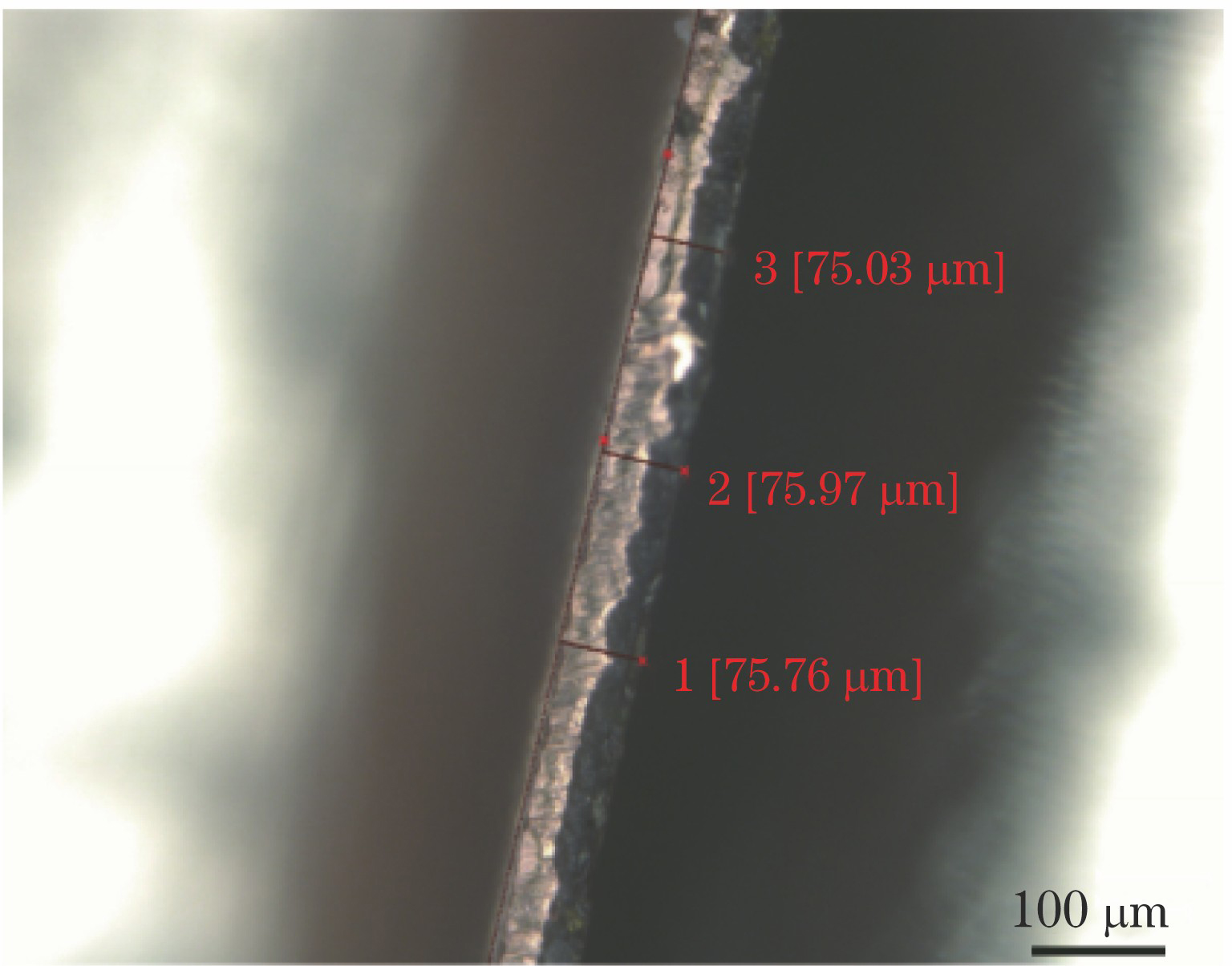
Fig. 1. Ultra depth of field measurement results of FPC copper-clad laminate
Fig. 2. Experimental scheme
Fig. 3. FPC copper etching model and scanning path
Fig. 4. Relationship among femtosecond laser power, depth, and roughness at the etched area of copper layer
Fig. 5. Relationship among femtosecond laser frequency, depth, and roughness in the etched area of copper layer
Fig. 6. Relationship among scanning speed of femtosecond laser, depth, and roughness in the etched area of copper layer
Fig. 7. Relationship among femtosecond laser scanning times, depth, and roughness in the etched area of the copper layer
Fig. 8. Relationship among femtosecond laser defocusing amount, depth, and roughness in the etched area of copper layer
Fig. 9. Measurement results of 3D laser microscope. (a) Etching window; (b) 3D morphology
Fig. 10. EDS measurement results of etched area. (a) Micro morphology of etched area; (b) EDS spectrum
Serial number | Power /mW | Scanning speed /(mm·s-1) | Frequency /kHz | Scanning times | Defocusing amount /mm | Etching depth /μm | Roughness /μm |
---|
1 | 70 | 30 | 30 | 3 | 0 | 20.04 | 1.39 | 2 | 170 | 30 | 30 | 3 | 0 | 23.62 | 1.54 | 3 | 270 | 30 | 30 | 3 | 0 | 31.94 | 1.77 | 4 | 370 | 30 | 30 | 3 | 0 | 67.57 | 2.23 | 5 | 470 | 30 | 30 | 3 | 0 | Through | Through | 6 | 370 | 30 | 20 | 3 | 0 | 55.43 | 1.45 | 7 | 370 | 30 | 40 | 3 | 0 | 33.02 | 2.15 | 8 | 370 | 30 | 50 | 3 | 0 | 28.80 | 2.01 | 9 | 370 | 30 | 60 | 3 | 0 | 23.32 | 1.89 | 10 | 370 | 40 | 30 | 3 | 0 | 32.73 | 2.01 | 11 | 370 | 50 | 30 | 3 | 0 | 28.32 | 1.85 | 12 | 370 | 60 | 30 | 3 | 0 | 26.82 | 1.72 | 13 | 370 | 70 | 30 | 3 | 0 | 24.17 | 1.65 | 14 | 370 | 30 | 30 | 1 | 0 | 23.08 | 1.84 | 15 | 370 | 30 | 30 | 2 | 0 | 30.66 | 2.04 | 16 | 370 | 30 | 30 | 4 | 0 | Through | Through | 17 | 370 | 30 | 30 | 5 | 0 | Through | Through | 18 | 370 | 30 | 30 | 3 | 0.3 | 42.87 | 2.03 | 19 | 370 | 30 | 30 | 3 | 0.15 | 48.15 | 2.14 | 20 | 370 | 30 | 30 | 3 | -0.15 | 69.77 | 2.97 | 21 | 370 | 30 | 30 | 3 | -0.3 | Through | Through |
|
Table 1. Process parameters and experimental results of FPC copper laminate etched by femtosecond laser
Level | Average power /mW | Scanning speed /(mm·s-1) | Scanning times | Defocusing amount /mm | Repetition frequency /kHz |
---|
1 | 280 | 36 | 1 | 0.12 | 35.0 | 2 | 294 | 37 | 2 | 0.18 | 36.5 | 3 | 308 | 38 | 3 | 0.24 | 38.0 | 4 | 322 | 39 | 4 | 0.30 | 39.5 |
|
Table 2. Factor level table
Serial number | Level | Depth /μm | Roughness /μm |
---|
A | B | C | D | E |
---|
1 | 1 | 1 | 1 | 1 | 1 | 21.15 | 1.28 | 2 | 1 | 2 | 2 | 2 | 2 | 30.10 | 1.57 | 3 | 1 | 3 | 3 | 3 | 3 | 31.40 | 1.60 | 4 | 1 | 4 | 4 | 4 | 4 | 73.08 | 1.19 | 5 | 2 | 1 | 2 | 3 | 4 | 30.46 | 1.56 | 6 | 2 | 2 | 1 | 4 | 3 | 15.77 | 1.51 | 7 | 2 | 3 | 4 | 1 | 2 | 69.23 | 1.37 | 8 | 2 | 4 | 3 | 2 | 1 | 29.62 | 1.67 | 9 | 3 | 1 | 3 | 4 | 2 | Through | Through | 10 | 3 | 2 | 4 | 3 | 1 | Through | Through | 11 | 3 | 3 | 1 | 2 | 4 | 14.87 | 1.50 | 12 | 3 | 4 | 2 | 1 | 3 | 25.97 | 1.85 | 13 | 4 | 1 | 4 | 2 | 3 | Through | Through | 14 | 4 | 2 | 3 | 1 | 4 | 39.22 | 2.48 | 15 | 4 | 3 | 2 | 4 | 1 | 32.46 | 1.67 | 16 | 4 | 4 | 1 | 3 | 2 | 16.01 | 1.34 |
|
Table 3. Element arrangement and results of orthogonal test
Item | Level average | Power /mW | Scanning speed /(mm·s-1) | Scanning times | Defocusing amount /mm | Frequency /kHz |
---|
Depth | k1 | 38.93 | 50.70 | 16.95 | 38.89 | 39.71 | k2 | 36.27 | 40.17 | 29.75 | 37.55 | 47.73 | k3 | 48.01 | 36.99 | 45.96 | 38.37 | 37.18 | k4 | 40.82 | 36.17 | 73.37 | 49.23 | 39.41 | Range | 11.74 | 14.53 | 56.42 | 11.68 | 10.55 | Roughness | k1 | 1.41 | 1.42 | 1.41 | 1.75 | 1.54 | k2 | 1.53 | 1.85 | 1.66 | 1.58 | 1.43 | k3 | 1.68 | 1.54 | 1.92 | 1.50 | 1.65 | k4 | 1.83 | 1.51 | 1.28 | 1.46 | 1.68 | Range | 0.42 | 0.43 | 0.64 | 0.29 | 0.25 |
|
Table 4. Range analysis
Area | Atomic number fraction /% |
---|
C | O | Cu |
---|
Original FPC board layer | 0.2 | 1.1 | 98.7 | Etched bottom area | 74.3 | 24.9 | 0.2 |
|
Table 5. Atomic number fraction of each element