Abstract
Confocal Raman microscopy is currently used for label-free optical sensing and imaging within the biological, engineering, and physical sciences as well as in industry. However, currently these methods have limitations, including their low spatial resolution and poor focus stability, that restrict the breadth of new applications. This paper now introduces differential-confocal controlled Raman microscopy as a technique that fuses differential confocal microscopy and Raman spectroscopy, enabling the point-to-point collection of three-dimensional nanoscale topographic information with the simultaneous reconstruction of corresponding chemical information. The microscope collects the scattered Raman light together with the Rayleigh light, both as Rayleigh scattered and reflected light (these are normally filtered out in conventional confocal Raman systems). Inherent in the design of the instrument is a significant improvement in the axial focusing resolution of topographical features in the image (to ), which, when coupled with super-resolution image restoration, gives a lateral resolution of 220 nm. By using differential confocal imaging for controlling the Raman imaging, the system presents a significant enhancement of the focusing and measurement accuracy, precision, and stability (with an antidrift capability), mitigating against both thermal and vibrational artefacts. We also demonstrate an improved scan speed, arising as a consequence of the nonaxial scanning mode.1. INTRODUCTION
Over the last four decades, conventional confocal Raman microscopy (CRM) has attracted considerable interest by providing a method of generating both two- and three-dimensional chemical mapping, creating images that have come to be called “molecular fingerprints.” The current methods combine the characteristics of Raman spectroscopy with the topographic imaging of confocal microscopy, enabling analytical applications in materials [1–3], biomedical sciences [4–6], and physical chemistry [7–9]. There are, however, a number of limitations associated with the technique. For example, these microscopes have been designed by using a single optical path for both topographic and Raman mapping or imaging. Since the intensity of Raman scattered light is ca. times weaker than that of Rayleigh scattered light, in order to obtain good signal-to-noise ratio, the size of the pinhole used in creating the confocal image has typically been significantly larger ( hundreds of micrometers) in diameter than the focused beam at the pinhole, thereby limiting the microscopes’ resolution. Where smaller pinholes have been used to improve this aspect of the performance, this has resulted in a decrease in the Raman signal intensity.
The need to use a large pinhole in current microscopes also leads to a poor focus sensitivity near the focal point of the confocal system’s axial response curve and thus reduces the precision and accuracy of the axial focus in CRM; see Fig. 1. Furthermore, conventional CRMs have a low lateral image resolution [10].
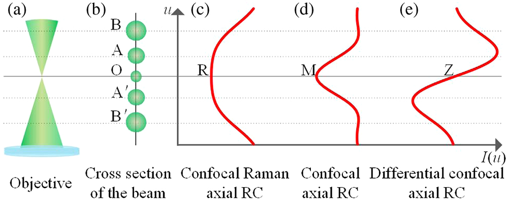
Figure 1.Laser beam focus. (a) The laser beam is focussed at O. (b) Cross section of the beam at positions A, and B, away from the focus; (c) confocal axial response curve for a conventional CRM, where R is the position of maximum intensity, corresponding to the focus position O; (d) confocal axial response curve for a confocal microscope, where, again, M is the maximum position of the curve corresponding to the focus O; (e) differential confocal axial response curve, where the zero-crossing position Z, of the curve corresponds to the focus O. In (c)–(e), is the normalized axial coordinate and is the axial response intensity. RC, response curve.
Alternative implementations of CRM, developed to improve the spatial resolution, have either used phase plates to reduce the point spread function (PSF) [11], structured light confocal Raman spectroscopy [12,13] to compress the excitation spot, or super-resolution image restoration confocal Raman spectroscopy [14,15]. These techniques have practical limitations, including the complexity of the instrumentation, the nature of the samples that can be studied, and fluctuations in the signal levels during point-by-point imaging. Typically, these iterations in the design have led to a reduction in the range of applications to which they can be applied. Importantly, the techniques described above [11–15] also either decrease the spectral excitation efficiency due to the significant reduction in excitation light intensity, and/or rely upon image postprocessing techniques, which in themselves do not improve the inherent spatial resolution.
Sign up for Photonics Research TOC. Get the latest issue of Photonics Research delivered right to you!Sign up now
In addition to having low spatial resolution, conventional CRMs are affected by poor long-term focus stability. This is particularly important in Raman imaging, since again, as a direct consequence of the low intensities of the scattered light being collected, point-excited, point-detected Raman mapping of a surface may take several hours [16]. This relatively slow data acquisition rate is due in part to the low Raman signal intensity and in part to the detector readout rates. As a consequence, given the requirement that image acquisition must be performed by scanning either axially (layer by layer), or laterally (point by point), the possibility of drift in the system caused by environmental factors, such as thermal fluctuations, low frequency mechanical vibrations, or gravity is greatly increased, often leading to image defocusing.
Notwithstanding these physical limitations, the collection of high-resolution and high-precision images to provide both chemical and topographic mapping simultaneously remains an important challenge across the engineering, physical, chemical, and biomedical sciences [17–19]. As a consequence, the combinations of scanning probe microscopy (SPM) and Raman scattering [20–27], including atomic force microscopy (AFM)-Raman, scanning near-field optical microscopy (SNOM)-Raman, and tip-enhanced Raman spectroscopy (TERS), have been used to successfully achieve accurate chemical and topographic mapping with excellent lateral resolutions of as small as 0.3–15 nm. However, unlike far-field optical methods including those used for Raman microscopies (see Fig. 1), these probe-based techniques require coupling of a scanned probe and laser, making it difficult to achieve accurate in situ topographic and Raman measurements. In addition, such measurements cannot be performed for samples with high aspect ratios.
In this paper, we now present differential-confocal controlled Raman microscopy (DCCRM) as an innovative fusion of differential confocal microscopy and Raman spectroscopy that not only significantly improves the axial focusing resolution but also enhances both the stability and speed of scanning [28]. We also implement a super-resolution image restoration technology to improve the lateral resolution of the performance of DCCRM for topographic imaging. To enable this, we not only collect the scattered Raman light but also capture both the Rayleigh light and reflected light (which are normally abandoned in existing confocal Raman systems).
The differences between conventional CRM and DCCRM are illustrated by the characteristic axial response curves for both techniques in Figs. 1(c) and 1(e). We also provide a schematic illustration of the light path for DCCRM in Fig. 2, showing the use of separate optical paths optimized for both the Raman scattered light and the Rayleigh light (including the Rayleigh scattering and reflected light). This details how the Rayleigh light is split into two optical paths that pass through separate confocal pinholes situated symmetrically above and below the focus of a corresponding imaging lens (labelled PL, Fig. 2), providing a differential measurement of the variation in the Rayleigh light intensity with axial distance . By using the same excitation source coupled with simultaneous detection from the two light pathways, we ensure that there is a point-to-point (synchronous) correspondence of microdomain topography (with high spatial resolution) and chemical information (at close to the theoretical resolution). Importantly, by removing the need for axial scanning to maintain focus, the technique also provides faster scanning speeds with the necessary focus stability, required to acquire high-fidelity three-dimensional images.

Figure 2.Differential-confocal controlled Raman microscopy. (a) Schematic of DCCRM where PH is the pinhole, NPBS (R/T: 2/8) and (R/T: 5/5) are the nonpolarizing beam splitters, PL is the pinhole lens, and RL is the Raman lens. (b) The differential confocal sensing curve, where is the normalized axial coordinate, illustrating the linear characteristic of the response of over the interval .
2. METHOD
A. Differential-Confocal Controlled Raman Microscopy
As stated, the DCCRM system [Fig. 2(a)] comprises a differential confocal system (as the reflected light path from the notch filter) and a confocal Raman spectroscopy system (as the transmitted path through the notch filter). The Rayleigh light and Raman scattered light arriving from the sample are split using a notch filter, with the Rayleigh light (which is not usually used in a conventional CRM) entering a differential confocal system.
As a consequence of the high Rayleigh light intensity, two small pinholes (10 μm in diameter) are arranged, with one placed in front of the focal plane and one behind the focal plane (with the same offset). This arrangement was used to construct a differential confocal system, enabling highly accurate and precise axial focusing for both the Rayleigh light and Raman scattered light from the same excitation source, and a theoretical lateral resolution improvement of 1.2-fold, compared with using a single large pinhole optimized for the confocal Raman system [10]. Simultaneously, Raman scattered light enters the confocal Raman spectroscopy system, enabling synchronized Raman imaging, topographic imaging, and focus tracking. Interestingly, we note that an extra mirror can also be added between the nonpolarizing beam splitter (NPBS) and the notch filter to adjust the angle of the notch filter, so providing opportunities for different applications that may include studies on polarization or low wavenumber analysis.
The DCCRM spectroscopy system enables two detection modes: a zero-cross trigger mode and a nonaxial scanning mode. In the zero-cross trigger mode, the differential confocal curve (Fig. 2) is obtained. Here the zero-crossing point of the differential confocal curve accurately corresponds to the focus of the objective [28]. High-accuracy focus positioning can be achieved, with the minimum position of the focal spot accurately captured, leading to an improved spatial resolution.
To understand the nonaxial scanning mode, we show [Fig. 2(b)] the magnitude of the sensing signal of the DCCRM system, with the confocal curves and and their corresponding output signals and . The sensing curve and the sensing signal are shown as Fig. 2(b) and Eq. (1), respectively, with the sensing function being generated from the curve fitting of the differential confocal curve of the DCCRM system (the sensing interval shows a linear characteristic). Note that the use of can eliminate the impact of multiplicative noise on differential signal. This enables the sample height to be calculated according to Eq. (2):
Thus, for samples with low aspect ratios, with topography within the range of the depth of focus, chemical mapping can be carried out using the nonaxial scanning mode.
The sensing characteristics of DCCRM are such that the technique only requires scanning of one layer to reconstruct the image. This leads to a significant increase in the scanning speed, when compared to conventional CRM, which often requires “multilayer” scanning. For samples where peak-to-trough heights extend beyond the depth of focus we use focus tracking to extend the range of the nonaxial scanning mode, further enhancing our large-area, fast scanning capability.
In addition, we also implemented a maximum posterior algorithm based upon the Poisson–Markov model (MPMAP) [29], enabling image restoration to improve the lateral resolution, as detailed in our previous study [30]. The iterative kernel of this algorithm is shown in Eq. (3): where * is a correlation operator, is the degraded image, is the target image, is the system PSF, is the balance factor, is a step factor that controls the convergence behavior and speed of the algorithm, is the energy function within the Geman–McClure model where a penalty function is used, and and refer to pixel index.
B. Laser Differential-Confocal Controlled Raman Microscope
As stated, in our DCCRM, pinholes and [Fig. 2(a)] are placed either side of the focus plane of the pinhole lens, enabling us to implement a laser differential-confocal controlled Raman microscope. A diode-pumped solid-state (DPSS) laser (532 nm, Samba, Colbolt, Sweden) was used as the excitation source, with a 100× objective (, Olympus, Japan). A piezo-actuated objective scanner (P-725, Physik Instrumente, Germany) was used to perform axial scanning and focusing, with two 10 μm pinholes (PH-10, Newport, USA) to construct the differential confocal system.
The Rayleigh light and Raman light were separated with the notch filter (LPD01-532RU-25, Semrock, USA) shown in Fig. 2(a). A spectrometer (Tianjin Gangdong Technology Co., Ltd., LRS-5) equipped with a CCD (DU-416 A-LCD-DD, Andor, UK) was used for collecting the Raman signal. The sample was mounted on an piezo-motorized stage (P-542.2CD, Physik Instrumente, Germany) to enable scanning. Data were collected on a bespoke Visual Studio 2010 program written in C++ and were exported into MATLAB for analysis and display.
C. Sample Characterization
To demonstrate the resolution, accuracy, and precision of the system, model metrology samples were used including a standard etched calibration grating (TGXYZ02, Mikromasch) and an aluminum mirror (GCC-102102, Daheng Optics, China). The standard grating consisted of a Si substrate and a overlayer, with height of 100 nm, patterned with 5 μm periodic lines. The sample was also characterized by AFM measurements as a gold-standard reference (Dimension 3100 Atomic Force Microscope, Veeco, USA); Fig. 3.
Figure 3.Axial focusing resolution measurements. Result of axial focusing resolution measurement (a) in the differential confocal configuration and (b) in the confocal Raman configuration; (c) 3D profile of the standard grating. (d) Comparison of the cross-sectional profile obtained with DCCRM, with image restoration (SDCCRM) and with AFM of the standard grating in (c), in which the DCCRM profile was extracted from data marked by the red arrow in (c).
In order to verify the antidrift capability of the system, we also used a custom-made grating to compare the performance of Raman scanning in CRM and DCCRM modes. This sample was fabricated on a Si substrate with an overlayer of 135 nm thick aluminum patterned with 5 μm periodic lines. During the experiments, the stage was stepped by 3 μm, with scanning sizes of and , scanning steps of 400 nm; Fig. 4. Finally, in order to show the application of the DCCRM, synchronous Raman mapping with topographical imaging was performed on an MX84521FP chip, with an , scanning range of and a scanning step of 150 nm. Samples were also characterized by AFM.
Figure 4.Antidrift measurements using our custom-made grating sample to perform Raman scanning in CRM and DCCRM modes. (a) Antidrift measurement in CRM mode, measured as the normalized Raman intensity with a step of 3 μm at point A. There is a fall in the normalized Raman intensity due to an abrupt sample defocusing event; (b) complementary results showing antidrift measurement in DCCRM mode. The same step in the stage occurred at position B, although there was no defocusing with no consequent decrease in the normalized Raman intensity. During the experiments, the stage was stepped at points A and B. The scanning sizes were , and the , scanning step was 400 nm. Note: Raman intensity is normalized.
3. RESULTS
A. Spatial Resolution Performance
Initially, the aluminum mirror was used to characterize the axial focusing resolution of the system. The objective lens was adjusted to the focus (determined by the zero point in the differential confocal response curve) and the objective was then moved in 1 nm steps in the axial direction, driven by the piezo-actuated objective scanner. The signal obtained by the differential confocal system is shown in Fig. 3(a). As the objective is gradually defocused, the signal intensity reduced, giving a clear step profile with an axial focusing resolution of . Similarly, for the Raman imaging system a custom grating sample was characterized. Again, the objective was moved to the focus setting as the zero point, and the objective moved in steps of 100 nm axially, driven by the piezo-actuated objective scanner. The signal obtained by the confocal Raman system Fig. 3(b), clearly shows the step profile, indicating a spectral axial focusing resolution of the system of at least 100 nm.
In addition, the topography of the standard grating (details in the Sample Characterization section) was measured at steps of 100 nm over an range of ; see Fig. 3(c). The measured height of the sample was estimated as by the DCCRM system, with the corresponding height measured by AFM being ; Fig. 3(d).
We also employed an MPMAP image restoration algorithm, the results of which are shown as the green curve in Fig. 3(d). Figure 3(d) also shows the comparison of DCCRM, implementing image restoration (SDCCRM) and AFM for the same cross-sectional profile extracted from the row indicated by the red arrow in Fig. 3(c) (where is in the range of 10%–90% of the receding profile). The horizontal distance from the DCCRM system (red) was measured as 265 nm; that distance (green) was improved to 220 nm using the image restoration method, while that of AFM (blue) was 157 nm. The results illustrate that with image restoration, the lateral resolution of DCCRM for topographic imaging is .
B. Antidrift Performance
Traditional optical confocal microscopes provide the highest optical resolution (the intensity of the reflected light has a maximum at the focus with relatively small changes in intensity if the sample is slightly closer or further from the objective). However, such instruments are unable to unequivocally recognize and compensate for any defocus due to drift (for example, software-based drift compensation algorithms rely upon taking a series of intensity measurements at different axial distances to find the “sharpest” image). This phenomenon is shown in Fig. 1(d), where the maximal nature of the intensity-defocus position plot means that simply measuring the value of the intensity gives no indication of the direction of defocus at points near the maximum, making its use as an error signal in focusing problematic.
In order to compensate for drift, we designed a system where the sample was continuously (actively) repositioned so that the optical image stayed in focus at the same place in the field of view of the imaging camera. We verified the antidrift capability of the system using a custom-made grating sample (details supplied in the Sample Characterization section) to perform Raman scanning in CRM and DCCRM modes, respectively; see Figs. 4(a) and 4(b). It can be seen from Fig. 4(a) that since the CRM cannot operate focus tracking, the system becomes disturbed by a “step” at point A. The image becomes defocused and, as a consequence, the Raman intensity suddenly drops by and the lateral spatial resolution also becomes worse. Figure 4(b) shows comparable results for imaging in DCCRM mode, where the differential confocal system for focus tracking results in the image staying in focus regardless of the sudden movement of the stage with no apparent axial “jump” nor a step change in the profile within the axial direction—with the resulting image being consistent with the actual sample topology.
C. Topographic Imaging and Raman Mapping Reconstruction Performance
Within semiconductor device fabrication, following the optimization of a manufacturing process for a chip or device, the geometry, composition, and stress of the microstructured materials are assessed (as these often determine both lifetime and performance). In situ topographic imaging and chemical mapping of such semiconductor structures is thus of great significance for quality assurance, as this detailed analysis provides insight into both the working and failure mechanisms (with the overall aim of improving fabrication yields and lifetime). As an illustration, we used DCCRM to image the MX84521FP chip, commonly used in home computing and shown in Fig. 5.
Figure 5.Topographic imaging and Raman mapping of the DCCRM system. (a) Photographic microscopic image; (b) topographic image; (c) single Raman spectrum; (d) distribution of material composition map; (e) shift of the Raman peak map; and (f) a topographic image (in , , ) and Raman map (in colors) merged. The , scanning range is , with a scanning step of 150 nm.
Figure 5(a) shows a photomicrograph of the chip with the red dotted line enclosing the region of interest (ROI), relating to Fig. 5(b), as the corresponding topographic information obtained using DCCRM. Figure 5(c) shows the Raman spectrum of the chip at point C, within the ROI. The spot size was ca. 1 μm and was focused on a point that has both polymer composite used in packaging (with a Raman peak at ) and silicon (). Figure 5(d) shows a map of the distribution of material composition based upon these two Raman peaks at (green) and (magenta).
Information concerning the stress and strain within layers within the chip can also be obtained through the analysis of the peak shifts in the Raman spectra [Fig. 5(e)], enabling stress and strain distributions to be calculated, according to Eq. (4) [31–34]: where is the change in Raman shift, and are the phonon deformation potentials (PDPs) of silicon, and are elements of the compliance tensor of silicon, is the Raman shift of stress-free silicon, and is the stress. As stated, this knowledge can reveal important information for optimizing manufacturing protocols and for quality assurance by helping to predict failure mechanisms and quantify the stress between thin films used in the fabrication of multilayer integrated circuits.
As the DCCRM system uses the same excitation spot for Rayleigh light confocal imaging as it does for Raman scattering in the confocal Raman system, the topographic image precisely matches the distribution of material in the composition map, point by point. By merging the two maps [Fig. 5(f)], a composite image containing information on both the topographic information [in , , , with measured as the height in micrometers (μm)] and the material composition (in colors) can be obtained [where magenta represents the distribution of silicon, green represents the polymer composite, and white is the mixed region where both polymer and silicon are present, e.g., point C in Fig. 5(a)]. By using Rayleigh light for accurate axial focusing, the drift in the system is sufficiently buffered from environmental disturbance, meaning that the image is always in focus, without introducing errors due to defocusing, despite the image taking to collect.
4. DISCUSSION
Conventional CRM is traditionally configured with a single optical path both for the topographic imaging and Raman detection. In order to collect sufficient Raman signals, such microscopes use a large pinhole, leading to poor focus sensitivity and reduced axial and lateral resolution [10]. We demonstrate that we can improve the performance of confocal Raman by using the technique of differential confocal microscopy, which we combine with confocal Raman spectroscopy to enhance scan speed, spatial resolution, and to provide an antidrift ability.
In contrast to the use of a static single pinhole in a conventional confocal microscope or CRM, we split the Rayleigh light from the sample through two independent small pinholes, one placed in front of the focal plane and one behind the focal plane (with the same offset). By combing the two signals from these pinholes we can measure the optical defocus of the signal and either use it directly as a measure of the topography of the sample or as an error signal for closed-loop mechanical adjustment of focus.
When the two signals are combined and the optical defocus of the signal is used as a measure of surface topography, this configuration enables a nonaxial scanning mode as shown in Fig. 3(c) for a grating structure with a depth of . The system also enables an alternative mode where we combine the two signals as an error signal for closed-loop mechanical adjustment of focus as shown in Fig. 4.
As stated, the technique not only has a strong antidrift capability but also shows a axial focusing resolution and fast speed, both demonstrated by stepping the objective scanner (Fig. 3) in an image collected in . We also show that we can simultaneously obtain topography and Raman data, including Raman shifts (Fig. 5). In the future this capability could be used to build images that quantify the stress between thin films and in process optimization during fabrication of multilayer integrated circuits [31–34]. Finally, we also note that in this current configuration, we have focused on improvement in axial drift, which, due to the influence of environmental factors, including gravity, vibration, and temperature, is most significant, in order to enable the quantitative analysis of the Raman signals. We propose that, in future work, we will also address the important topic of reducing lateral drift, which will have an impact on imaging of nanoscale features.
5. CONCLUSIONS
In conclusion, DCCRM enables the accurate and precise in situ Raman mapping combined with synchronous topographic imaging, providing high spatial resolution, fast scan speeds, and antidrift capability. The technique provides images rich in chemical information, opening up new applications in the physical and chemical sciences and biomedicine. DCCRM may also provide specific applications in materials engineering and quality assurance (including those in assessing material stress) where topographical imaging could be combined with the corresponding subsurface Raman data.
Acknowledgment
Acknowledgment. The authors gratefully thank Dr. Andrew Glidle and Prof. Jonathan Weaver at the University of Glasgow for useful discussions. Prof. Jonathan Cooper acknowledges the support of the Overseas Expertise Introduction Project for Discipline Innovation (B18005) in enabling this collaboration.
References
[1] P. Kun, G. Kukucska, G. Dobrik, J. Koltai, J. Kürti, L. P. Biró, L. Tapasztó, P. Nemes-Incze. Large intravalley scattering due to pseudo-magnetic fields in crumpled graphene. npj 2D Mater. Appl., 3, 11(2019).
[2] T. Ukmar-Godec, L. Bertinetti, J. W. Dunlop, A. Godec, M. A. Grabiger, A. Masic, H. Nguyen, I. Zlotnikov, P. Zaslansky, D. Faivre. Materials nanoarchitecturing via cation–mediated protein assembly: making limpet teeth without mineral. Adv. Mater., 29, 1701171(2017).
[3] X. Zhou, X. Hu, B. Jin, J. Yu, K. Liu, H. Li, T. Zhai. Highly anisotropic GeSe nanosheets for phototransistors with ultrahigh photoresponsivity. Adv. Sci., 5, 1800478(2018).
[4] G. J. Puppels, F. F. M. De Mul, C. Otto, J. Greve, M. Robert-Nicoud, D. J. Arndt-Jovin, T. M. Jovin. Studying single living cells and chromosomes by confocal Raman microspectroscopy. Nature, 347, 301-303(1990).
[5] N. Altangerel, G. O. Ariunbold, C. Gorman, M. H. Alkahtani, E. J. Borrego, D. Bohlmeyer, P. Hemmer, M. V. Kolomiets, J. S. Yuan, M. O. Scully. In vivo diagnostics of early abiotic plant stress response via Raman spectroscopy. Proc. Natl. Acad. Sci. USA, 114, 3393-3396(2017).
[6] S. Pal, A. Ray, C. Andreou, Y. Zhou, T. Rakshit, M. Wlodarczyk, M. Maeda, R. Toledo-Crow, N. Berisha, J. Yang, H. Hsu, A. Oseledchyk, J. Mondal, S. Zou, M. F. Kircher. DNA-enabled rational design of fluorescence-Raman, bimodal nanoprobes for cancer imaging and therapy. Nat. Commun., 10, 1926(2019).
[7] M. Y. Huang, H. G. Yan, T. F. Heinz, J. Hone. Probing strain-induced electronic structure change in graphene by Raman spectroscopy. Nano Lett., 10, 4074-4079(2010).
[8] D. R. Klein, D. MacNeill, Q. Song, D. T. Larson, S. Fang, M. Xu, R. A. Ribeiro, P. C. Canfield, E. Kaxiras, R. Comin, P. Jarillo-Herrero. Enhancement of interlayer exchange in an ultrathin two-dimensional magnet. Nat. Phys., 15, 1255-1260(2019).
[9] W. Dai, F. Shao, J. Szczerbiński, R. McCaffrey, R. Zenobi, Y. Jin, A. D. Schlüter, W. Zhang. Synthesis of a two-dimensional covalent organic monolayer through dynamic imine chemistry at the air/water interface. Angew. Chem., 55, 213-217(2016).
[10] T. Wilson, A. R. Carlini. Three-dimensional imaging in confocal imaging systems with finite sized detectors. J. Microsc., 149, 51-66(1988).
[11] R. D. Frankel. Dipole-like backscatter stimulated Raman scattering for in vivo imaging. J. Raman Spectrosc., 45, 764-772(2014).
[12] K. Hamada, K. Fujita, N. I. Smith, M. Kobayashi, Y. Inouye, S. Kawata. Raman microscopy for dynamic molecular imaging of living cells. J. Biomed. Opt., 13, 044027(2008).
[13] K. Watanabe, A. F. Palonpon, N. I. Smith, L. D. Chiu, A. Kasai, H. Hashimoto, S. Kawata, K. Fujita. Structured line illumination Raman microscopy. Nat. Commun., 6, 10095(2015).
[14] L. Duponchela, P. Milanfar, C. Ruckebusch, J. Huvenne. Super-resolution and Raman chemical imaging: from multiple low resolution images to a high resolution image. Anal. Chim. Acta., 607, 168-175(2008).
[15] J. P. Smith, F. C. Smith, J. Ottaway, A. E. Krull-Davatzes, B. M. Simonson, B. P. Glass, K. S. Booksh. Raman microspectroscopic mapping with multivariate curve resolution-alternating least squares (MCR-ALS) applied to the high-pressure polymorph of titanium dioxide, TiO2-II. Appl. Spectrosc., 71, 1816-1833(2017).
[16] R. W. Havener, A. W. Tsen, H. C. Choi, J. Park. Laser-based imaging of individual carbon nanostructures. NPG Asia Mater., 3, 91-99(2011).
[17] W. Bao, M. Melli, N. Caselli, F. Riboli, D. S. Wiersma, M. Staffaroni, H. Choo, D. F. Ogletree, S. Aloni, J. Bokor, S. Cabrini. Mapping local charge recombination heterogeneity by multidimensional nanospectroscopic imaging. Science, 338, 1317-1321(2012).
[18] H. J. Cho, K. W. Oh, C. H. Ahn, P. Boolchand, T.-C. Nam. Stress analysis of silicon membranes with electroplated permalloy films using Raman scattering. IEEE Trans. Magn., 37, 2749-2751(2001).
[19] P. J. Caspers, G. W. Lucassen, G. J. Puppels. Combined in vivo confocal Raman spectroscopy and confocal microscopy of human skin. Biophys. J., 85, 572-580(2003).
[20] M. Anderson. Locally enhanced Raman spectroscopy with an atomic force microscope. Appl. Phys. Lett., 76, 3130-3132(2000).
[21] F. De Angelis, G. Das, P. Candeloro, M. Patrini, M. Galli, A. Bek, M. Lazzarino, I. Maksymov, C. Liberale, L. Claudio Andreani, E. Di Fabrizio. Nanoscale chemical mapping using three-dimensional adiabatic compression of surface plasmon polaritons. Nat. Nanotechnol., 5, 67-72(2010).
[22] N. Hayazawa, Y. Inouye, Z. Sekkat, S. Kawata. Metallized tip amplification of near-field Raman scattering. Opt. Commun., 183, 333-336(2000).
[23] J. Toporski, T. Dieing, T. Dieing, O. Hollricher. Resolution and performance of 3D confocal Raman imaging systems. Confocal Raman Microscopy, 121-153(2018).
[24] N. Anderson, A. Hartschuh, S. Cronin, L. Novotny. Nanoscale vibrational analysis of single-walled carbon nanotubes. J. Am. Chem. Soc., 127, 2533-2537(2005).
[25] J. Stadler, T. Schmid, R. Zenobi. Nanoscale chemical imaging using top-illumination tip-enhanced Raman spectroscopy. Nano Lett., 10, 4514-4520(2010).
[26] T. Yano, P. Verma, Y. Saito, T. Ichimura, S. Kawata. Pressure-assisted tip-enhanced Raman imaging at a resolution of a few nanometers. Nat. Photonics, 3, 473-477(2009).
[27] S. Jiang, Y. Zhang, R. Zhang, C. Hu, M. Liao, Y. Luo, J. Yang, Z. C. Dong, J. G. Hou. Distinguishing adjacent molecules on a surface using plasmon-enhanced Raman scattering. Nat. Nanotechnol., 10, 865-869(2015).
[28] W. Q. Zhao, H. Cui, L. R. Qiu, Y. Wang. Laser differential confocal mapping-spectrum microscopic imaging method and device. U.S. patent(2015).
[29] B. Su, W. Jin. POCS-MPMAP based super-resolution image restoration. Acta Photon. Sin., 32, 502-504(2003).
[30] H. Cui, W. Zhao, Y. Wang, Y. Fan, L. Qiu, K. Zhu. Improving spatial resolution of confocal Raman microscopy by super-resolution image restoration. Opt. Express, 24, 10767-10776(2016).
[31] V. T. Srikar, A. K. Swan, M. S. Unlu, B. B. Goldberg, S. M. Spearing. Micro-Raman measurement of bending stresses in micromachined silicon flexures. J. Microelectromech. Syst., 12, 779-787(2003).
[32] F. Ureña, S. H. Olsen, J. P. Raskin. Raman measurements of uniaxial strain in silicon nanostructures. J. Appl. Phys., 114, 144507(2013).
[33] E. Anastassakis, A. Cantarero, M. Cardona. Piezo-Raman measurements and anharmonic parameters in silicon and diamond. Phys. Rev. B, 41, 7529-7535(1990).
[34] W. A. Brantley. Calculated elastic constants for stress problems associated with semiconductor devices. J. Appl. Phys., 44, 534-535(1973).

