Abstract
Both the coarse wavelength division multiplexing and LAN-WDM receiver optical sub-assemblies (ROSAs) were developed. The ROSA package was hybrid integrated with a planar lightwave circuit arrayed waveguide grating (AWG) with 2% refractive index difference and a four-channel top-illuminated positive-intrinsic-negative photodetector (PD) array. The output waveguides of the AWG were designed in a multimode structure to provide flat-top optical spectra, and their end facet was angle-polished to form a total internal reflection interface to realize vertical coupling with a PD array. The maximum responsivity of ROSA was about 0.4 A/W, and its 3 dB bandwidth of frequency response was up to 20 GHz for each transmission lane. The hybrid integrated ROSA would be a cost-effective and easy-assembling solution for 100 GbE data center interconnections.With the rapid growth of data center interconnection, high speed, low cost, and compact optical transmitting and receiving devices are massively required[1]. Therefore, several 100 GbE criteria have been standardized for such demands[2,3]. These standards defined four transmission lanes to achieve high transmission rates by using wavelength division multiplexing (WDM) technology, where each lane would have a bit rate of 25 Gb/s for the 100 GbE applications. There are two commonly used wavelength allocations in correspondence to the International Telecommunication Union (ITU) standards, which are called coarse WDM (CWDM) and LAN-WDM. Their channel spacings are 20 and 4.5 nm (800 GHz), respectively.
Usually the free-space structure of using thin-film filters (TFFs) is assembled as a de-multiplexer (deMUX) in both CWDM and LAN-WDM due to its relatively flat spectral profile and low insertion loss[4,5]. However, the difficulties of making TFF deMUX are associated to its complex optical axis alignment and optical reliability. Furthermore, with the increase of data rates in the near future, more transmission lanes will be indispensably needed in deMUX devices[6,7]. The planar lightwave circuit (PLC) technology, especially the arrayed waveguide grating (AWG) deMUX[8,9], will have greater potential over the bulky TFFs devices, since PLC demonstrated wafer-level manufacturability, wavelength accuracy, and channel scalability[10].
In this article, we present both CWDM and LAN-WDM receiver optical sub-assembly (ROSA) packages using silica-based PLC AWG, in which multimode output waveguides are adopted to provide a flat-top spectral profile[11]. The end facet of output waveguides of AWG is polished to a 40° angle. The polished facet is used as a reflection mirror instead of an optical prism[12], flip-chip bonding[13] or vertically mounting photodetectors (PDs)[14] to turn the light direction and realize a simple optical coupling between the output waveguides and Si-Ge PD[15] array. The direct coupling greatly simplified the packaging process and reduced the manufacturing cost without using an extra coupling lens. The hybrid integrated ROSA packages show high linearity and reach maximum responsivity over 0.4 A/W. With channel scalability and an advanced modulation format [e.g., pulse amplitude modulation (PAM4)], it will be very promising to be employed in optical transceivers for high speed applications.
Sign up for Chinese Optics Letters TOC. Get the latest issue of Chinese Optics Letters delivered right to you!Sign up now
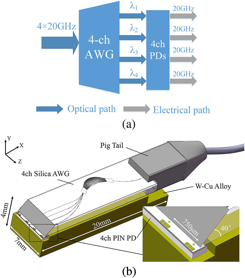
The schematic of the ROSA is shown in Fig. 1(a). On the receiving side, the light signal was divided into four lanes with individual wavelengths after passing through the AWG deMUX. The four PDs of an array collected the individual light signals to transform them into electrical signals, in which the intensity modulation and directed detection (IM-DD)[16] operated. IM-DD is a common and low-cost method in short-range interconnection. With this configuration, a designed ROSA package is shown in Fig. 1(b), and it consisted of a four-channel silica-based AWG chip and a four-channel top-illuminated positive-intrinsic-negative (PIN) PD array. The end facet of the AWG output side was polished to 40°, forming a reflection mirror for the lensless coupling. The light was totally internally reflected out of the end facet and directly coupled to the PD sensing area. Because of its excellent thermal and electrical conductivity, the W85Cu15 alloy coated with Au was chosen as the chip carrier. Moreover, its thermal expansion coefficient is close to Si–Ge material. The ROSA is in the size of , which is compact enough to be implemented in carrier frequency pulse (CFP)/CFP2/CFP4 modules.

Figure 1.Configuration of ROSA. (a) Circuit diagram. (b) Package schematic.
Different from the common AWG devices whose input and output waveguides were single-mode, the output waveguides of the AWG chip in our ROSA packages were with a multimode structure and had a broad flat-top spectral profile[11]. The flat-top profile provides a much wider tolerance to wavelength drift, which is caused by direct modulation (frequency chirp)[17], operating temperature changes[18], etc. With its 2.0% ultra-high refractive index contrast, the silica-based rectangle waveguide core is able to make more compact devices compared to that with an index contrast of 0.75% and 1.5%. Considering the optical fiber coupling loss and manufacturability, the silica waveguides were designed with a core of 4 μm in height. We simulated the relationship between the effective refractive index of different modes and waveguide widths and showed them in Fig. 2. Both wavelengths of 1271 and 1331 nm were chosen in our simulation, since they were the shortest and the longest wavelengths specified in the Institute of Electrical and Electronics Engineers (IEEE) 802.3ba standard. All other wavelengths between 1271 and 1331 nm were covered and had the same mode quantity.
Figure 2.Relationship between the effective refractive index () and waveguide width.
From the simulation results, we chose 4 and 11.5 μm as the widths of single-mode and multimode waveguides, respectively. The multimode waveguides with this width can support four modes, as seen in Fig. 2.
In order to assemble the ROSA package with an AWG chip more easily than building a waveguide-type PD[19,20] in hybrid integration, the normal top-illuminated Ge/Si PIN PD array is used, whose sensing area is 20 μm in diameter, responsivity is up to 0.9 A/W@-3 V, and dark current is typically 150 nA@-3 V.
Because the PD array’s illumination area is on top, and the light transmission direction in AWG waveguides is horizontal, the light turning component is vital to light coupling between the AWG and PDs. For simplicity, the output end facet of the AWG chip was ground at a certain angle to turn the light direction into the PD. The three-dimensional (3D) finite-difference time-domain (FDTD) method was adopted to simulate the turning structure, as shown in Fig. 3.
Figure 3.Longitudinal section of propagation simulation with an angle of 40°.
Four monitors were set in the simulation with the transmission distances of 0, 10, 20, and 30 μm away from the top side of the AWG to collect the light power and show the spot profiles. The light power declines with increase of the transmission distance displayed in Fig. 4(a). The other angles were also simulated, as shown in Fig. 4(b). More power can be reflected by the mirror as the angle is decreased. The turning efficiency is sensitively related with the angle value.
Figure 4.Transmission loss (a) at different distances and wavelengths under the 40° angle and (b) at different angles and wavelengths under 20 μm distance. (The simulated light source contains both the polarizations simultaneously.)
Another concern would be the beam spot profile for the finite sensing area of the PD. If the beam profile is expanded too much, which may exceed the sensing area, the PD cannot collect all of the light, and this will lead to extra loss and reduce the receiving efficiency. The beam spot profiles are simulated and displayed in Fig. 5.
Figure 5.Spot profiles under the 20 μm transmission distance at (a) 45°, (b) 42°, (c) 40°, and (d) 38°.
Figure 5 shows that the spot profile is expanded severely with the decrease of the turning angle. At 20 μm distance, the long side of the profile is about 20 μm when the turning angle is 40°. There is a trade-off issue between the turning efficiency and the receiving efficiency. To obtain the higher turning efficiency, a smaller angle is preferred, but this angle will lead the beam profile to expand more and make the receiving efficiency lower. Contrarily, if the angle is increased to acquire higher receiving efficiency, the turning efficiency will be reduced. The final compromise tuning angle of 40° was chosen for the optimal turning efficiency, and the distance between the top side of the AWG and the PD array would be less than 20 μm to have a lower loss.
The AWG chip was fabricated on the silica platform. The lower silica cladding was grown first on the Si substrate by thermal oxide. Then, the core silica layer was deposited by Ge-doped plasma-enhanced chemical vapor deposition (PECVD). After that, the waveguide structure was etched by the inductively coupled plasma (ICP) etching process to form sharp and smooth edges. The last step was to again deposit the upper silica cladding by PECVD. The scanning electron microscope (SEM) photographs were taken to show the fabrication waveguides in Fig. 6.
Figure 6.SEM photographs of (a) single-mode waveguides and (b) a multimode waveguide.
To couple and align with the PD array more practically, the AWG chip would be flipped over so that the reflected light from output waveguides would only pass through the thin upper cladding. The 40° reflection mirror was made by three steps. First, the iron grinding wheel was used to roughly form the 40° angle. Second, the end face was polished with SiC particles in the size of 1 μm on an iron plate for about 30 min. In the last step, the abrasives were replaced with ceria of 0.5 μm diameter to polish for 30 min to get an ultra-fine facet as a reflection mirror that was extremely smooth and minimized the loss. The AWG chip and the PD array were actively aligned and coupled during the hybrid integration process. The PD array was mounted on the carrier by silver epoxy. The AWG chip was held and moved with a fixture toward the PD array until the PD generated a maximum photocurrent; then, the AWG chip was glued with UV glue. The ROSA’s photograph is shown in Fig. 7.
Figure 7.Photograph of ROSA.
The responsivity spectra of both CWDM and LAN-WDM ROSA are tested and shown in Fig. 8. The results were measured under the polarization random condition. The top of the spectra is box-like, and the maximum responsivity is up to 0.4 A/W@-3 V for both. Considering the PD chip’s responsivity of 0.9 A/W, the optical loss is about 3.5 dB, which comes from 1.5 dB transmission loss of the AWG, 0.65 dB coupling loss between the AWG and PD (considering both the TE and TM modes), and 1 dB loss of pig tail (connector between the AWG and fiber) to the AWG. Practically, the coupling loss between the AWG and PD could be higher due to the reflection mirror defect and assembling error. The gray regions in Fig. 8 represent the wavelength range of four lanes defined in the IEEE 802.3ba standard. It is obvious that the measured spectra totally cover the grid range for all lanes. The 1 dB bandwidth of CWDM and LAN-WDN is wider than 15 and 3 nm, respectively, which is about 70% of the channel spectral spacing. Their optical crosstalk is less than , which provides high isolation between the adjacent channels. There is a little ripple at the top of spectra; it could be attributed to the tiny defects on the facet edge caused by polishing. Figure 9 shows the linearity of the CWDM and LAN-WDM ROSA. It reveals an ultra-high linearity of up to 4 mW, which is broad enough to meet the common non-return to zero (NRZ) modulation format. More important is that the high linearity will have a great potential in advanced modulation applications, such as PAM4 that uses four levels to double the bit rate and needs higher linearity of ROSA. The small signal electro-optical (E-O) frequency response (normalized) was also measured and shown in Fig. 10. The 3 dB bandwidth is up to 20 GHz for each lane and allows over 25 Gb/s transmission according to the factor of about 1.4 between an achievable bit rate (NRZ) and the bandwidth of the devices[21]. The ROSA packages with such a broad frequency response will be feasibly used for 100 GbE (NRZ) and 200 GbE (PAM4) applications.
Figure 8.ROSA responsivity in (a) CWDM and (b) LAN-WDM (gray areas indicate CWDM and LAN-WDM grid).
Figure 9.Linearity in CWDM and LAN-WDM.
Figure 10.Small signal frequency responses in CWDM and LAN-WDM.
The data showed that the performance of the ROSAs in this article basically reached the same level compared to the other works, including the responsivity, 1 dB bandwidth, crosstalk, and 3 dB bandwidth of the E-O response (or data rate).
In conclusion, both of the CWDM and LAN-WDM ROSAs were developed using PLC silica-based hybrid integrated technology. The optical coupling between the AWG with multimode output waveguides and the top-illuminated PIN PD was achieved directly by angle-polishing the end facet of the AWG chip. The angle facet could act as a total internal reflection interface without using any other extra optical parts. The responsivity of both the CWDM and LAN-WDM ROSA is as high as 0.4 A/W@-3 V. The 1 dB bandwidth of each single lane is about 70% of its optical channel spacing, and the optical spectra are flat-top. The optical crosstalk is less than , and the 3 dB bandwidth of the E-O frequency response is up to 20 GHz for all signal lanes. This cost-effective and easy-assembling technology will be hopefully used in not only 100 GbE but also 400 GbE systems with more transmission lanes and advanced modulation format.
| Type | Responsivity (A/W) | 1 dB Bandwidth (nm) | Crosstalk (dB) | 3 dB E-O Response (GHz) |
|---|
| CWDM in Ref. [13] | 0.3−0.4 | >10 | <−20 | >9 |
| Our work | 0.4 | >15 | <−20 | 20 |
| LAN-WDM in Ref. [14] | ∼0.5 | >2.5 | <−30 | 25 (Gb/s) |
| Our work | 0.4 | >3 | <−20 | 20 |
Table 1. Performance Comparison of ROSAs
References
[1] P. Bernasconi, L. Buhl, D. T. Neilson, J. H. Sinsky, N. Basavanhally. IEEE Photon. Technol. Lett., 24, 1657(2012).
[2] IEEE P802.3ba 40Gb/s and 100Gb/s Ethernet task force(2010).
[3] D. Lewis, C. Cole. CWDM4 MSA technical specifications rev 1.1(2015).
[4] S. K. Kang, J. K. Lee, J. C. Lee, K. Kim. Proceedings of 2010 Electronic Components and Technology Conference, 2001(2010).
[5] K. Mochizuki, H. Itamoto, H. Aruga, K. Akiyama, Y. Horiguchi, S. Nishikawa, M. Nakaji, R. Takemura, A. Sugitatsu. Proceedings of 2010 15th Optoelectronics and Communications Conference, 242(2010).
[6] C. Ferrari, C. Bolle, M. A. Cappuzzo, R. Keller, F. Klemens, Y. Low, N. Basavanhally, A. R. Papazian, F. Pardo, M. P. Earnshaw. Proceedings of European Conference on Optical Communication(2014).
[7] Z. Zhao, Y. Liu, Z. Zhang, X. Chen, J. Liu, N. Zhu. Chin. Opt. Lett., 14, 120603(2016).
[8] H. Dai, J. An, Y. Wang, J. Zhang, L. Wang, H. Wang, J. Li, Y. Wu, F. Zhong, Q. Zha. J. Semicond., 35, 104010(2014).
[9] C. Li, X. Qiu, X. Li. Photon. Res., 5, 97(2017).
[10] K. Takada, M. Abe, M. Shibata, M. Ishii, K. Okamoto. IEEE Photon. Technol. Lett., 13, 1182(2001).
[11] M. R. Amersfoort, C. R. Deboer, F. P. G. M. Vanham, M. K. Smit, P. Demeester, J. J. G. M. Vandertol, A. Kuntze. Electron. Lett., 30, 300(1994).
[12] F. Nakajima, M. Kawamura, K. Oki. Proceedings of IEEE Photonics Conference, 305(2013).
[13] Y. Doi, T. Ohyama, T. Hashimoto, S. Kamei, A. Ohki, M. Ishii, M. Yanagisawa, S. Mino. Conference on Lasers and Electro-Optics(2004).
[14] J. K. Lee, Y. S. Jang. Proceedings of International Conference on Information & Communication Technology Convergence, 758(2015).
[15] B. Cheng, C. Li, Z. Liu, C. Xue. J. Semicond., 37, 081001(2016).
[16] Z. Zhao, J. Liu, Y. Liu, N. Zhu. J. Semicond., 38, 121001(2017).
[17] P. M. Anandarajah, R. Maher, L. P. Barry, A. Kaszubowska-Anandarajah, E. Connoly, T. Farrell, D. McDonald. IEEE Photon. Technol. Lett., 20, 72(2008).
[18] J. W. Pan, J. I. Chyi. IEEE J. Quantum Electron., 32, 2133(1996).
[19] D. Yin, T. He, Q. Han, Q. Lü, Y. Zhang, X. Yang. J. Semicond., 37, 114006(2016).
[20] J. M. Lee, M. K. Kim, W. Y. Choi. Chin. Opt. Lett., 15, 100401(2017).
[21] G. G. Mekonnen, W. Schlaak, H. G. Bach, R. Steingruber, A. Seeger, T. Engel, W. Passenberg, A. Umbach, C. Schramm, G. Unterborsch, S. van Waasen. IEEE Photon. Technol. Lett., 11, 257(1999).