• Chinese Optics Letters
  • Vol. 19, Issue 7, 071901 (2021)
Chenguang Xin1、2、3、*, Jie Qi1、2, Rui Zhang1、2, Li Jin1、2, and Yanru Zhou4、**
Author Affiliations
  • 1Academy for Advanced Interdisciplinary Research, North University of China, Taiyuan 030051, China
  • 2School of Instrument and Electronics, North University of China, Taiyuan 030051, China
  • 3State Key Laboratory of Modern Optical Instrumentation, College of Optical Science and Engineering, Zhejiang University, Hangzhou 310027, China
  • 4School of Information and Communication Engineering, North University of China, Taiyuan 030051, China
  • show less
    DOI: 10.3788/COL202119.071901 Cite this Article Set citation alerts
    Chenguang Xin, Jie Qi, Rui Zhang, Li Jin, Yanru Zhou. In-situ modal inspection based on transverse second harmonic generation in single CdS nanobelt[J]. Chinese Optics Letters, 2021, 19(7): 071901 Copy Citation Text show less
    CdS NBs. (a) Scanning electron microscope image of upper face (scar bar, 1 µm). (b) Scanning electron microscope image of side face (scar bar, 5 µm). (c) Optical microscope image (scar bar, 10 µm).
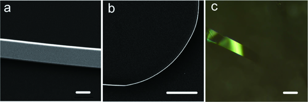
    Fig. 1. CdS NBs. (a) Scanning electron microscope image of upper face (scar bar, 1 µm). (b) Scanning electron microscope image of side face (scar bar, 5 µm). (c) Optical microscope image (scar bar, 10 µm).
    Schematic diagram of the experiment. CdS NB is placed across a slit of two MgF2 to avoid influence from substrates.
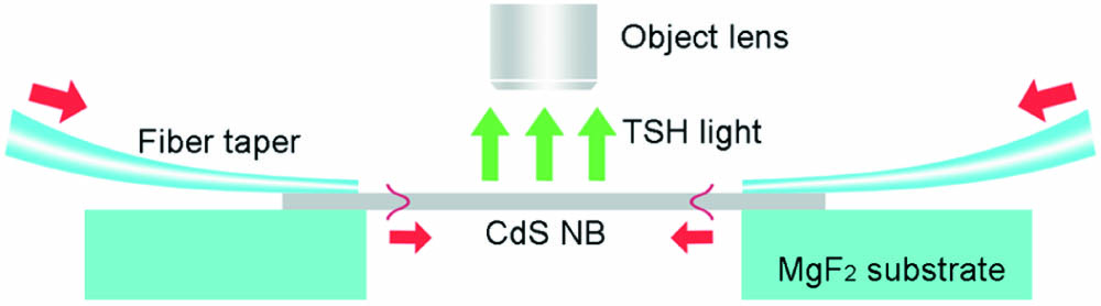
    Fig. 2. Schematic diagram of the experiment. CdS NB is placed across a slit of two MgF2 to avoid influence from substrates.
    Emitting angle determined by the phase matching condition.
    Fig. 3. Emitting angle determined by the phase matching condition.
    (a) Optical microscope image of a 2-µm-wide CdS NB with a height of 200 ± 10 nm (scar bar, 50 µm). Inset shows simulated profiles of the fundamental and second-order modes inside an NB at a wavelength of 1064 nm (scar bar, 1 µm). In the FDTD simulation, the width is 2 µm, and the height is 200 nm. (b) TSH interference patterns for the CdS NB with 1064 nm CW light input. (c) Optical microscope image of a 300 nm diameter nanowire (scar bar, 50 µm). Inset shows simulated profile of the first and second-order modes at a wavelength of 1064 nm (scar bar, 300 nm). In the simulation, the nanowire has a hexagonal cross section, which agrees with the reality. The side-to-side diameter is 300 nm. (d) TSH patterns for the nanowire with 1064 nm CW light input.
    Fig. 4. (a) Optical microscope image of a 2-µm-wide CdS NB with a height of 200 ± 10 nm (scar bar, 50 µm). Inset shows simulated profiles of the fundamental and second-order modes inside an NB at a wavelength of 1064 nm (scar bar, 1 µm). In the FDTD simulation, the width is 2 µm, and the height is 200 nm. (b) TSH interference patterns for the CdS NB with 1064 nm CW light input. (c) Optical microscope image of a 300 nm diameter nanowire (scar bar, 50 µm). Inset shows simulated profile of the first and second-order modes at a wavelength of 1064 nm (scar bar, 300 nm). In the simulation, the nanowire has a hexagonal cross section, which agrees with the reality. The side-to-side diameter is 300 nm. (d) TSH patterns for the nanowire with 1064 nm CW light input.
    (a) Measured spectrum of TSH signal. (b) Intensity of the TSH signal with different input power. (c) Extracted intensity profile for the TSH signal along the axis of the NB, corresponding to the inside image of Fig. 4(b). (d) Corresponding FFT spectrum. The arrows indicate the first five peaks in the spectrum.
    Fig. 5. (a) Measured spectrum of TSH signal. (b) Intensity of the TSH signal with different input power. (c) Extracted intensity profile for the TSH signal along the axis of the NB, corresponding to the inside image of Fig. 4(b). (d) Corresponding FFT spectrum. The arrows indicate the first five peaks in the spectrum.
    Δneff and D with different surrounding refractive indices. Inside image shows calculated effective index for the fundamental mode and the second-order mode, respectively. The width of the NB is 2 µm.The height of the NB is 200 nm. The pumping wavelength is 1064 nm.
    Fig. 6. Δneff and D with different surrounding refractive indices. Inside image shows calculated effective index for the fundamental mode and the second-order mode, respectively. The width of the NB is 2 µm.The height of the NB is 200 nm. The pumping wavelength is 1064 nm.
    (a) Δneff and D with different widths of NBs. The pumping wavelength is 1064 nm. (b) Δneff and D at different wavelengths for a 2-µm-wide CdS NB. The height of the NB is 200 nm.
    Fig. 7. (a) Δneff and D with different widths of NBs. The pumping wavelength is 1064 nm. (b) Δneff and D at different wavelengths for a 2-µm-wide CdS NB. The height of the NB is 200 nm.
    No.ModesΔneffPeriod (µm)Calculated Frequency (µm−1)Experimental Data (µm−1)
    11st & 2nd0.05569.530.1050.100
    22nd & 3rd0.09605.520.1810.225
    31st & 3rd0.15163.490.2860.299
    42nd & 4th0.23852.220.4500.424
    51st & 4th0.29421.800.5550.524
    Table 1. Comparison between Calculated Results of Modal Interference and Experimental Resultsa
    No.ModesModal Interference (µm−1)
    190 nm200 nm210 nm
    11st & 2nd0.1060.1050.104
    22nd & 3rd0.1830.1810.179
    31st & 3rd0.2890.2860.283
    42nd & 4th0.4550.4500.445
    51st & 4th0.5620.5550.549
    Table 2. Calculated Results of Modal Interference with Different Heights of NBs
    Chenguang Xin, Jie Qi, Rui Zhang, Li Jin, Yanru Zhou. In-situ modal inspection based on transverse second harmonic generation in single CdS nanobelt[J]. Chinese Optics Letters, 2021, 19(7): 071901
    Download Citation