
Qifan Zhu, Yuegang Fu, Zhiying Liu. Narrow-Band Polarization Notch Filtering of Visible Light Spectra Based on Photonic Crystal with Periodic Rectangular Holes[J]. Acta Optica Sinica, 2018, 38(12): 1223001
- Acta Optica Sinica
- Vol. 38, Issue 12, 1223001 (2018)
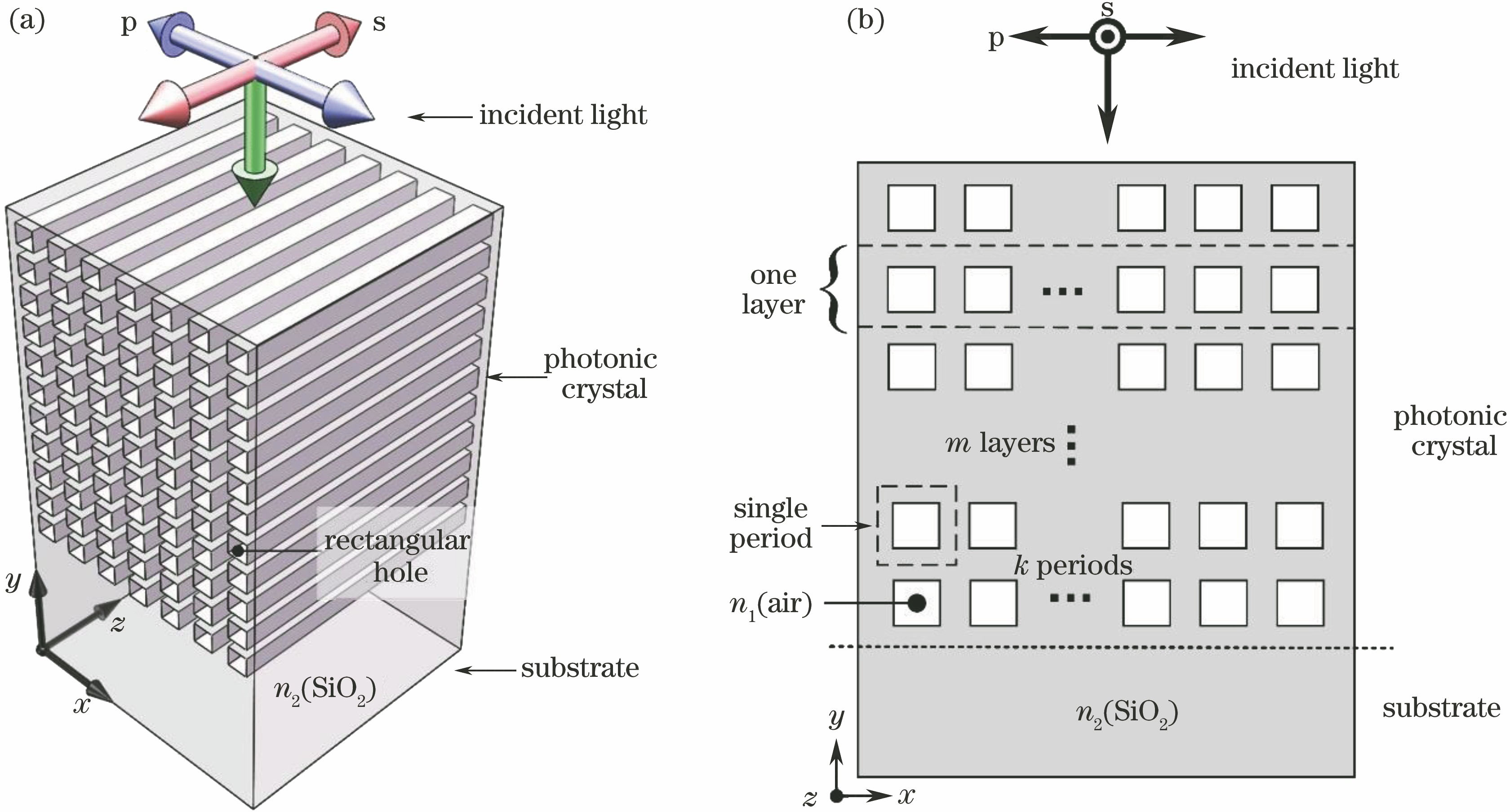
Fig. 1. Schematic of photonic crystal with periodic rectangular holes. (a) Three-dimensional model; (b) two-dimensional model in x-y plane
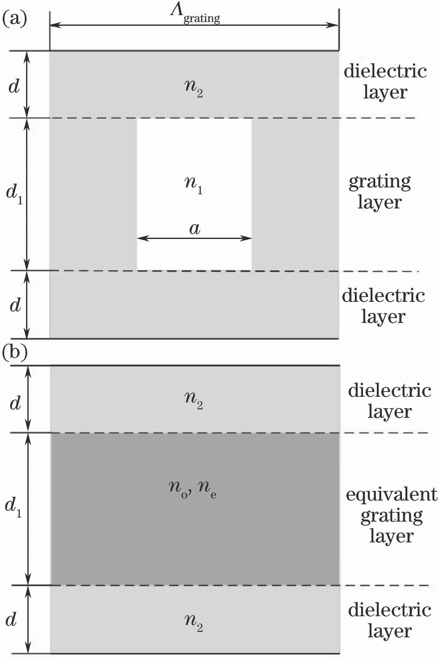
Fig. 2. Schematic of model. (a) Singly periodic structure; (b) equivalent layered structure
Fig. 3. Equivalent refractive index versus filling ratio f of grating layer
Fig. 4. Notch filtering features of visible light spectra versus filling ratio f of grating layer and wavelength. (a) s polarization; (b) p polarization
Fig. 5. Notch filtering features of visible light spectra versus thickness d and wavelength. (a) p polarization; (b) s polarization
Fig. 6. Notch filtering features of visible light spectra with central wavelengths of 435, 485, 535, 585, 635, 685 nm versus filling ratio f
Fig. 7. Transmittance at central wavelength versus periodic layer number m when filling ratios are 0.1, 0.2, 0.3, 0.4, 0.5, 0.6, 0.7, 0.8, 0.9. (a) p polarization; (b) s polarization
Fig. 8. Notch filtering features of visible light spectra under different central wavelengths. (a) 417 nm; (b) 497 nm; (c) 582 nm; (d) 685 nm
| |||||||||||||||||||||||||||||||||||||||||||||||||||||||
Table 1. Notch filtering band widths for p polarization and s polarization when filling ratios f are 0.37, 0.5, 0.75 and central wavelengths are different nm
| ||||||||||||||||||||||||||||||||||||||||||||||||||||||||||||||||||||||||||||
Table 2. Layer number, notch band width B and minimum transmittance Tmin for p polarization and s polarization under different filling ratios

Set citation alerts for the article
Please enter your email address
© Copyright 2018-2021 | Chinese Laser Press. All Rights Reserved 沪ICP备15018463号-20