
Yuan Yuan, Wayne V. Sorin, Di Liang, Stanley Cheung, Yiwei Peng, Mudit Jain, Zhihong Huang, Marco Fiorentino, Raymond G. Beausoleil. Mechanisms of enhanced sub-bandgap absorption in high-speed all-silicon avalanche photodiodes[J]. Photonics Research, 2023, 11(2): 337
- Photonics Research
- Vol. 11, Issue 2, 337 (2023)
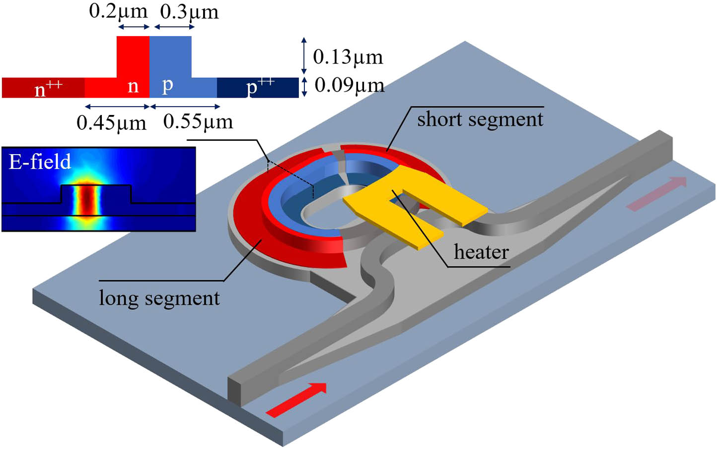
Fig. 1. Schematic diagram of the Ge-free MRR APD.
![(a) Measured normalized transmission spectrum at zero bias voltage. (b) Schematic of an MRR device. (c) Simulated coupling coefficient with the 1310 nm TE mode light [38].](/richHtml/prj/2023/11/2/337/img_002.jpg)
Fig. 2. (a) Measured normalized transmission spectrum at zero bias voltage. (b) Schematic of an MRR device. (c) Simulated coupling coefficient with the 1310 nm TE mode light [38].
Fig. 3. Simulated (a) electric field and (b) energy band diagrams of the Si PN junction at different bias voltages.
Fig. 4. Measured 2D colormaps of responsivity versus reverse-bias voltage and wavelength with bus WG power at (a) − 4.5 dBm
Fig. 5. Measured (a) total and dark currents, (b) wavelength, and (c) responsivity at resonance with bus WG power at − 4.5
Fig. 6. Measured and fitted photocurrent and responsivity versus bus WG power at reverse bias of (a), (b) − 4 V − 6.4 V
Fig. 7. (a) Simulated avalanche gain versus bias voltage at 0.1 mW. (b) Fitted avalanche gain versus optical power at − 6.4 V
Fig. 8. (a) Measured S11 response of the MRR APD at bias voltage of − 3 V − 6 V − 6.4 V − 6 V
Fig. 9. (a) Measured O-E S21 response at resonance. Measured eye diagrams of (b) 80 Gb/s NRZ and (c) 100 Gb/s PAM4 modulations with 6.5 dBm optical power in the bus WG at bias voltage of − 6.4 V
Fig. 10. Calculated responsivity of the all-Si straight waveguide with 1 mW input optical power at − 6.4 V
|
Table 1. Symbol Meanings, Values, and Units for the MRR APD Absorption Model

Set citation alerts for the article
Please enter your email address
© Copyright 2018-2021 | Chinese Laser Press. All Rights Reserved 沪ICP备15018463号-20