
Risheng Cheng, Sihao Wang, Chang-Ling Zou, Hong X. Tang. Design of a micrometer-long superconducting nanowire perfect absorber for efficient high-speed single-photon detection[J]. Photonics Research, 2020, 8(8): 1260
- Photonics Research
- Vol. 8, Issue 8, 1260 (2020)
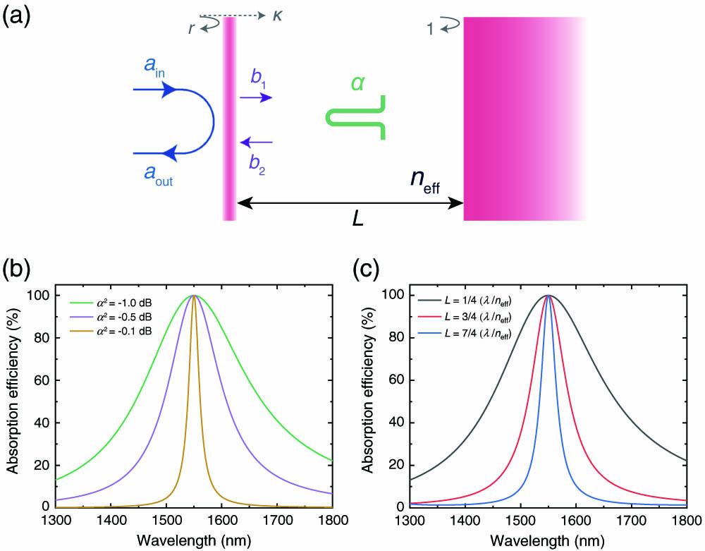
Fig. 1. One-side cavity model and calculated absorption efficiency of the nanowire absorber. (a) Schematic of the lossy cavity with an embedded nanowire absorber; (b) calculated nanowire absorption spectrum for varying photon loss per round trip in the cavity. The cavity length is fixed at L = 1 / 4 ( λ / n eff ) α 2 = − 1.0 dB
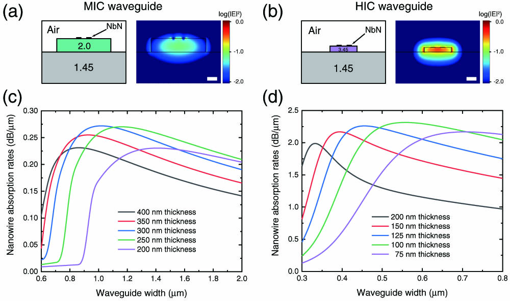
Fig. 2. Comparison between HIC and MIC waveguides. Cross-sectional schematics and simulated mode profiles of (a) MIC and (b) HIC waveguides. Scale bars, 200 nm; simulated nanowire absorption rates as a function of waveguide width for (c) MIC and (d) HIC waveguides of varying thicknesses.
Fig. 3. Simulated nanowire absorption rates depending on the nanowire width and thickness for the optimized HIC waveguide design.
Fig. 4. Effect of the waveguide types and geometry on the nanowire absorption rates. Cross-sectional schematics of (a) air-cladding waveguide on SiO 2 SiO 2
Fig. 5. H0-type PhC cavity design and optimization. (a) Schematic illustration of the H0-type PhC cavity formed by slightly shifting two air holes away from their original positions. a r s Q i s / a a
Fig. 6. Nanowire absorber integrated with H0-type PhC cavity. (a) Schematic of the H0-type PhC cavity with front partial mirror consisting of two smaller air holes. (b) Schematic of the H0-type PhC cavity with two arc-shaped nanowires embedded inside. (c) Simulated coupling quality factor Q c Q a
|
Table 1. Summary and Comparison of SNSPDs with Different Device Structures

Set citation alerts for the article
Please enter your email address
© Copyright 2018-2021 | Chinese Laser Press. All Rights Reserved 沪ICP备15018463号-20