High-power semiconductor laser diodes emitting at approximately 976 nm are in high demand in Yb-doped fiber lasers (YDFL) because YDFLs exhibit strong absorption peaks at approximately 976 nm. Specifically, the absorption cross section is as strong as three times that at a wavelength of approximately 915 nm. Thus, by using lasers with an emission wavelength of approximately 976 nm for optical pumping, the length of the active fiber can be significantly shortened, leading to cost savings and reduced nonlinear effects. With the ongoing advancements in various industrial applications, the emitting power of high-power lasers increases from 12 W (about 10 years ago) to approximately 30 W. Beyond the high-power requirement, one of the most sought-after features of high-power lasers is their power conversion efficiency (PCE). A superior PCE results in higher optical power emission, enhanced reliability, and reduced system costs.
In this study, we demonstrate the design and fabrication of high-efficiency, high-power 976-nm lasers. The tests on our fabricated devices show that, at room temperature and under the continuous-wave (CW) operation condition, the power conversion efficiency (PCE) reaches as high as 72.4% when the injection current is 10 A. However, the efficiency decreases to 61.3% when the current rises to 30 A, at which the operating power is 29.4 W.
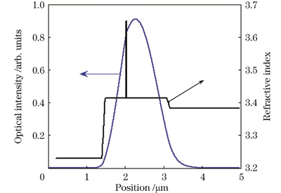
The epitaxy material is grown using the metal-organic chemical vapor deposition (MOCVD) method, and the structure contains an 8-nm-thick In0.175GaAs single quantum well (SQW) sandwiched between two separate confinement heterostructure (SCH) Al0.17GaAs layers. A wide optical cavity waveguide design is employed to reduce power density and cavity loss. The total thickness of the SCH layers is 1.5 μm. N-and P-doping are optimized to ensure the lasers produce the highest PCE when the emitting power is 25 W. Figure 1 shows the refractive index profile of our material structure, and Table 1 lists the detailed material structure.
After designing the material structure, we proceed with the optimization process to determine the optimum cavity length and anti-reflection (AR) reflectivity. In our optimization, we assume the aperture width is 200 μm, and the laser chip is mounted onto 350-μm-thick AlN ceramics in a P-side down manner, which, in turn, is mounted onto a copper block. Figure 3 displays the dependence of the laser parameters on the cavity length and the AR reflectivity. Based on this, it is clear that when the cavity length is in the range of 4?5 mm, a longer cavity yields better efficiency because the long cavity has a smaller series resistance and thermal impedance. Based on the theoretical simulation, we choose the cavity to be 5-mm-long, and the AR reflectivity is approximately 1%.
We conduct several material growth iteration processes to investigate the effect of growth conditions on device performance. Figure 4 shows the test results before growth optimization. In the figure, it can be observed that when tested at ambient temperature of 25 ℃ under the CW condition, the chip on sub-mount (COS) threshold current is approximately 1.2 A, slope efficiency is approximately 1.13 W/A, maximum PCE is 70.8% (corresponding optical power is 8.2 W). To further improve the device performance, we conduct growth optimization by optimizing the Al mole fractions for different layers in the structure, doping, and layer thickness.
The test results for the devices before and after growth optimization are shown in Fig. 6. Figure 5 shows the light-current curves and power conversion efficiencies under different test temperatures for chips with growth optimization. The highest PCE is 72.4% at a current of approximately 10 A. The efficiency reduces to 61.3% when the current reaches 30 A (the corresponding optical power is 29.4 W). Our devices appear to perform even better than those published in the literature. Figures 8 and 9 show the energy ratios under different slow-axis far-field divergence angles and lasing spectrum, respectively. In Fig. 8, it can be observed that more than 95% of the optical power is within horizontal far-field divergence angle of 9°, indicating good beam quality. The reliability, which is of critical importance for real-world applications, is also carefully evaluated by placing a number of devices in an accelerated lifetime test (Fig.10). Based on the lifetime test, there is no observable power degradation after 2000 h accelerated testing at an elevated temperature of 45 ℃.
In summary, we demonstrate the design and fabrication of high-efficiency, high-power 976-nm lasers. These devices are reliable and efficient. The PCE is as high as 72.4% at a current of 10 A; however, the efficiency decreases to 61.3% when the current reaches 30 A.