
Chen Wang, Yi-Hong Xu, Cheng Li, Hai-Jun Lin, Ming-Jie Zhao. Improved performance of Al/n+Ge Ohmic contact andGe n+/p diode by two-step annealing method [J]. Acta Physica Sinica, 2019, 68(17): 178501-1
- Acta Physica Sinica
- Vol. 68, Issue 17, 178501-1 (2019)
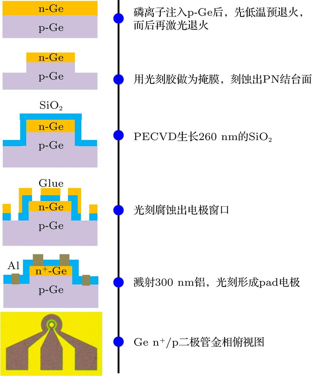
Fig. 1. Process flow used for the fabrication of Ge n+/p junction diodes.
Ge n+/p结二极管制备工艺流程图
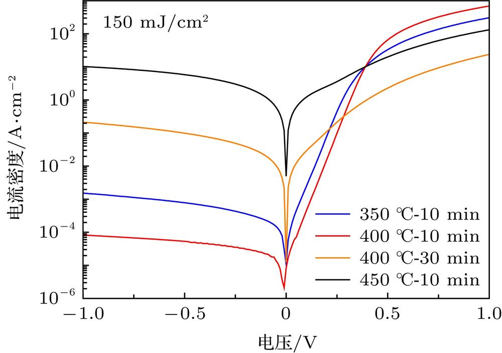
Fig. 2. Room temperature I -V characteristics of Ge n+/p junction diode formed by ELA with one pulse at 150 mJ/cm2 with different pre-annealing conditions.
150 mJ/cm2激光能量密度不同预退火条件下p-n结二极管的I -V 特性曲线
Fig. 3. Change of specific contact resistivity of Al/n+-Ge extracted by CTLM with different annealing conditions. The inset shows the CTLM schematic structure (top view).
Al/n+-Ge接触的比接触电阻率随不同退火条件的变化曲线, 内插图是CTLM结构的俯视图
Fig. 4. (a) Room temperature I -V characteristics of Ge n+/p junction diode; (b) rectification ratio of Ge n+/p junction diodes formed by ELA with or without pre-annealing at 400 ℃-10 min.
(a) 不同退火条件下Ge n+/p结二极管的I -V 特性曲线; (b) Ge n+/p结二极管的整流比随退火条件变化曲线
|
Table 1. Rectification ratio and ideality factor of Ge n+/p junction diodes under different annealing conditions.

Set citation alerts for the article
Please enter your email address
© Copyright 2018-2021 | Chinese Laser Press. All Rights Reserved 沪ICP备15018463号-20