Author Affiliations
1Wuhan National Laboratory for Optoelectronics, Huazhong University of Science and Technology, Wuhan 430074, China2Department of Electrical and Computer Engineering, McMaster University, Hamilton, ON L8S 4K2, Canadashow less
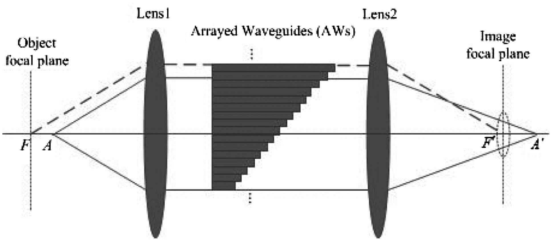
Fig. 1. Schematic diagram for illustration of the proposed structure: while the downstream signal (from F to F′) passes through a conventional AWG, the upstream signal (from F′ to A) sees an optical power (beam) combiner.
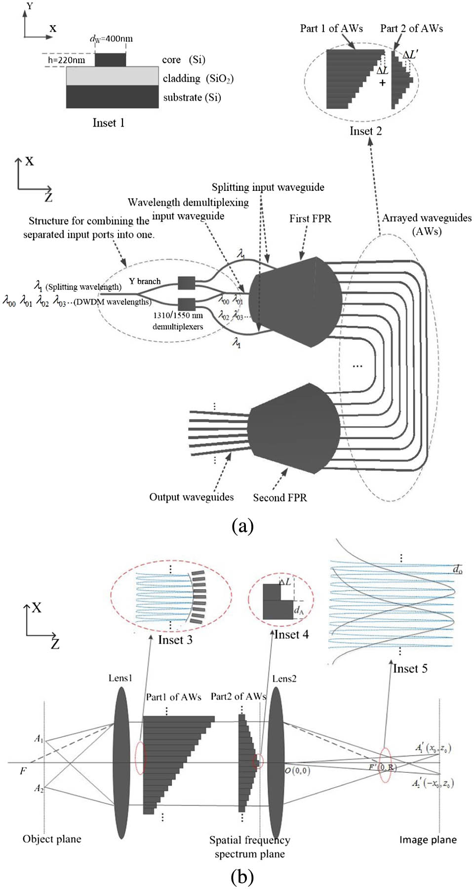
Fig. 2. (a) Schematic (top) view of the hybrid optical wavelength demultiplexer and power combiner; inset 1, cross-sectional view of the Si photonic wire; inset 2, a schematic (top) view of the equivalent AWs and the modifications. (b) Illustration of the proposed structure (excluding the structure for combing the separated input ports into one): while the downstream signal (from F to F′) passes through a conventional AWG, the upstream signal (from F′ to A1/A2) sees an optical power (beam) combiner; inset 3, field distribution with an interference pattern at the input port of the AWs for the upstream signal; inset 4, a zoomed-in view of part 2 of the AWs, where ΔL′ and dA are the equivalent unit length difference and unit width, respectively; inset 5, interference fringes at the output channels for the upstream signal, where dO is the interference fringe gap matching to the gap between the output waveguides.
Fig. 3. Electric field patterns in the (a) first FPR and (b) second FPR for the downstream signal at center wavelength λ0 when the device is working as a wavelength demultiplexer, and electric field patterns in the (c) first FPR and (d) second FPR for the upstream signal when the device is working as a power combiner.
Fig. 4. (a) Spectral response of the downstream wavelength demultiplexer and (b) the field distribution at output channels for the upstream optical power combiner at wavelength λ1=1303.3 nm.
Fig. 5. Spectral response of channels 23 to 27 (with noise) in the wavelength demultiplexer for the downstream signal.
Fig. 6. Field distribution (with noise) at the output channels of the upstream optical power combiner at wavelength λ1=1303.3 nm.
Material and Structural Parameters | Values | Silicon refractive index for | 3.476 | Silicon refractive index for | 3.503 | Silica refractive index for | 1.444 | Silica refractive index for | 1.447 | Output waveguide number | 32 | Array waveguide number | 95 | Output waveguide separation (μm) | 1.4 | Array waveguide separation (μm) | 2.4 | Input/Output/array waveguide width (μm) | 0.4 | Rowland circle diameter (μm) | 168.2 | Diffraction order | 23 | Free spectral range (FSR) (nm) | 30.6 | AW length difference (part 1) (μm) | 23.4 | AW length difference (part 2) (μm) | 1.0 | Splitting input waveguide position off demultiplexing input waveguide X (μm) | 19.8 | Splitting input waveguide position off demultiplexing input waveguide Z (μm) | 12.6 | Y branch angle (°) | 2 | 1310/1550-nm demultiplexers length (μm) | 312.0 | 1310/1550-nm demultiplexers width (μm) | 3.2 | Estimated whole device chip size () | |
|
Table 1. Material and Structural Parameters of the Device