Abstract
In this paper, we have proposed a hybrid optical wavelength demultiplexer and power combiner for a hybrid time- and wavelength-division multiplexing (TWDM) passive optical network (PON), i.e., a single passive optical device that functions as a wavelength demultiplexer for distributing the downstream signal in multiple wavelengths from the optical line terminal (OLT) to the optical network units (ONUs), and simultaneously as an power combiner for collecting the upstream signal in the same wavelength from the ONUs to the OLT. Through a design example of a 32 channel hybrid optical wavelength demultiplexer and power combiner on the silicon-on-insulator platform, our numerical simulation result shows that the insertion loss and adjacent channel crosstalk of the downstream wavelength demultiplexer are as low as 4.6 and , respectively, while the insertion loss and channel non-uniformity of the upstream power combiner can reach 3.5 and 2.1 dB, respectively. The proposed structure can readily be extended to other material platforms such as the silica-based planar lightwave circuit. Its fabrication process is fully compatible with standard clean-room technologies such as photo-lithography and etching, without any complicated and/or costly approach involved.1. INTRODUCTION
With the growing bandwidth demand for Internet and other bandwidth-hungry applications [1], there has been fast development for optical access technologies, such as fiber-to-the-home/curb (FTTH/FTTC) [2,3] networks, to overcome the bandwidth bottleneck. In the conventional time-division multiplexing (TDM) passive optical network (PON) [4], the bandwidth and optical power available to each optical network unit (ONU) are limited due to the splitting loss. Although the wavelength-division multiplexing (WDM) PON can overcome the limitation, in which each ONU is assigned to a specific wavelength, thus enjoying dedicated bandwidth, the high cost has limited its real-world deployment [5,6]. To achieve a proper balance between the performance and cost of PONs, a hybrid TDM/WDM (TWDM) PON [7–10] has been proposed as a promising solution for access networks in which WDM and TDM technologies are separately used for downstream and upstream transmissions, respectively. The asymmetric hybrid TWDM PON in which the download bandwidth is often much greater than the upload bandwidth, is suitable for much more intensive network service, such as high definition television and massive online games. In addition, for upstream transmission, identical low-cost transmitters with their wavelength set at 1310 nm can be adopted by all ONUs for cost minimizing [11].
As key components in the hybrid TWDM PON, the wavelength demultiplexer [12–14] for downstream transmission and the power combiner [15–17] for upstream transmission have been widely studied. However, the optical module based on multiple discrete components in separated downstream and upstream path design was bulky and not readily scalable with a large number of ONUs [11]. In this work, we have proposed a single passive optical device that can function as a wavelength demultiplexer for downstream signal transmission and simultaneously as an optical power combiner for upstream signal transmission. The silicon-on-insulator (SOI) waveguide has been chosen as the platform to show the device design idea. The proposed structure can be readily implemented on other material platforms, such as the silica-based planar lightwave circuit (PLC), depending on specific application requirements weighed by multiple factors, including bending and scattering losses, size and uniformity, processing ease, fabrication cost, and production yield. The working principle of the device is described briefly in Section 2. The device design is detailed in Section 3. We then show the numerical simulation results in Section 4, and have our work summarized in Section 5.
2. WORKING PRINCIPLE
To reach the wavelength demultiplexing function for the downstream signal, our proposed structure functions just as a conventional arrayed waveguide grating (AWG). The incident beam with multiple wavelengths propagating through the central input waveguide enters the first free propagation region (FPR) and becomes divergent. The divergent beam is then coupled into the waveguide array and propagates through the individual arrayed waveguides (AWs). As in the conventional AWs, the length difference between adjacent waveguides is fixed and equal to an integer multiple of the central wavelength of the demultiplexer: where is the effective index of the AW corresponding to wavelength . Through the AWs, light with different wavelength components experiences different phase delays, is consequently focused at different output positions by the diffraction of the second FPR, and is finally collected by different output waveguides.
Sign up for Photonics Research TOC. Get the latest issue of Photonics Research delivered right to you!Sign up now
For the upstream signal, however, the structure would work completely differently from an AWG; rather, it has to become a power (beam) combiner as required.
To explain the working principle of our proposed structure to the upstream signal, we abstract the AWG to a classical dual-lens imaging system, as shown in Fig. 1, where the lens pair 1 and 2 corresponds to the first and second FPR of the AWG, and the object and image focal planes correspond to the planes in which the input and output waveguides of the AWG are placed, respectively. The upstream signal wavelength is chosen as where is the aforementioned adjacent waveguide length difference of the AWs, is the effective index of the AWs corresponding to wavelength , and has a different integer value from . As such, we have ensured that the AWs have no effect on the upstream signal at wavelength , as it sees no phase delay at all.
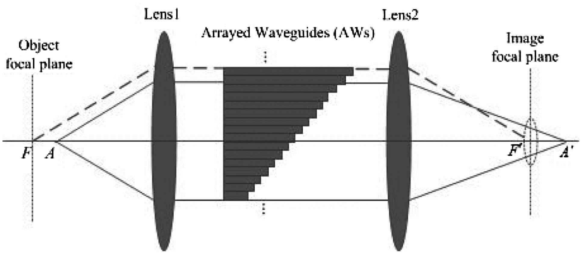
Figure 1.Schematic diagram for illustration of the proposed structure: while the downstream signal (from to ) passes through a conventional AWG, the upstream signal (from to ) sees an optical power (beam) combiner.
Next, following the relationship between the object–image focal planes, if the input light is launched at a position away from the object focal point on the optical axis (e.g., at point in Fig. 1), the output light will be focused at a position away from the image focal plane (i.e., at point in Fig. 1). Consequently, an expanded spot will be formed on the image focal plane where the output waveguides are placed for the downstream signal. If the expanded spot size can be designed to match the aperture size of the output waveguide array, an incident beam at a position away from the object focal plane can therefore be coupled into the output waveguides at the image focal plane, and we obtain a power (beam) splitter (at wavelength ). According to optical reciprocity, the upstream signal beams fed into the output waveguides will be combined at the input position by the same structure. Hence, we have a wavelength demultiplexer for the downstream signal at wavelength and a power (beam) combiner for the upstream signal at wavelength .
3. DEVICE DESIGN
Following the working principle explained above, we have designed a hybrid optical wavelength demultiplexer and power combiner (taking the 32 channel device as an example) on the SOI platform schematically shown in Fig. 2(a). The Si photonic wire with an air cladding is considered in this device, and the cross section is shown in inset 1 of Fig. 2(a). In the plane (top view), the whole device structure is based on a traditional AWG functioning as a wavelength demultiplexer for the downstream signal. However, modifications are introduced to incorporate the combiner design for the upstream signal aiming at not jeopardizing the wavelength demultiplexing performance.

Figure 2.(a) Schematic (top) view of the hybrid optical wavelength demultiplexer and power combiner; inset 1, cross-sectional view of the Si photonic wire; inset 2, a schematic (top) view of the equivalent AWs and the modifications. (b) Illustration of the proposed structure (excluding the structure for combing the separated input ports into one): while the downstream signal (from to ) passes through a conventional AWG, the upstream signal (from to ) sees an optical power (beam) combiner; inset 3, field distribution with an interference pattern at the input port of the AWs for the upstream signal; inset 4, a zoomed-in view of part 2 of the AWs, where and are the equivalent unit length difference and unit width, respectively; inset 5, interference fringes at the output channels for the upstream signal, where is the interference fringe gap matching to the gap between the output waveguides.
To make our explanation more clear without messing up the input and output waveguides in the device, we will turn the original power combiner for the upstream signal into an equivalent power splitter for the downstream signal at the same wavelength by following optical reciprocity. Hence, the device we are working on can be treated as a wavelength demultiplexer at center wavelength and a power splitter at wavelength , both for downstream signals with the same input and output ports.
In design of such a device structure, we first need to place the input port for the power splitter in front of that for the wavelength demultiplexer (AWG), according to the working principle of this power splitter (combiner) design explained in Fig. 1. However, a direct implementation of such an idea will need to insert a Si photonic wire inside the first FPR, which apparently wrecks the AWG. To solve this problem, we create a virtual input port for the power splitter by utilizing the beam interference effect, which, instead of inserting a Si photonic wire directly inside the FPR, allows us to place a pair of input Si photonic wires aside the FPR, without blocking the optical path of the AWG, as shown in Fig. 2(a). Following this arrangement, the input light for beam splitting (at wavelength ) will form a conventional bright–dark interference pattern at the exit of the first FPR, as shown in inset 3 of Fig. 2(b), which is then aligned to the discrete AWs with each interference fringe fitted into one AW. By noticing that the phase shift between adjacent fringes is , we will have to modify the phase condition given in above Eq. (2), to ensure that all fringes will be in phase after passing through the AWs, as required by the recombining and realigning of the fringes from the AWs to the output waveguides by the second FPR. The insertion position of the input port for the power splitter at the two symmetrical edges of the first FPR needs to be fine tuned for an exact matching between the period of the interference fringes and the separation of the AWs, which appears to be critical in reducing the insertion loss of the splitter (combiner) [18].
Second, the expanded spot at the image focal plane has its intensity following a Gaussian distribution along the lateral direction (), rather than a uniform distribution as required by an ideal splitter. To reduce the splitting non-uniformity among output channels, we have added an extra phase delay section to the conventional AWs, shown as part 2 and part 1, respectively, in inset 2 of Fig. 2(a). As shown by the drawing, the extra phase delay section (part 2) is actually a discrete prism that divides one beam into two equal portions. As such, the required interference fringes are formed in the image focal plane with their envelope flattened as a result of the superposition between the two offset Gaussian distributions. This effect is further illustrated in Fig. 2(b). The discrete prism still has to be designed in such a way that the period of its introduced interference fringes will match with the separation of the output waveguides. Actually, the top half part of the prism with its equivalent unit width and unit length difference , shown in inset 4 of Fig. 2(b), introduces a linear phase delay to a point in the exit plane of the prism , which also stands as the incident plane of lens 2. Consequently, it generates a corresponding spatial frequency shift at in the focal plane of lens 2. Its image point in the imagine plane must take the same spatial frequency and, thus, have its coordinates given by The same analysis applies to the bottom half of the prism, and we will have a symmetrical image point generated by a symmetrical point in the exit plane of the prism. The pair of image points in the image plane, as indicated by and in Fig. 2(b), will generate an interference pattern with its fringe gap given by matching to the gap between the output waveguides. By eliminating that corresponds to an arbitrarily selected point in the exit plane of the prism through Eq. (4), we find which links the prism’s design parameters ( and ) to the output waveguide gap () in the image focal plane as required.
Moreover, the extra phase delay brought in by the prism must have minimum effect on the AWG designed as the wavelength demultiplexer for the downstream signal. The length difference of the discrete prism is therefore chosen as so that the center wavelength component of the downstream signal experiences no extra phase delay at all, when passing through the inserted discrete prism.
Finally, we need to combine the separated input waveguides for the wavelength demultiplexer and power splitter into one general port, to form an in-line bi-directional device with 1-to- (downstream) and -to-1 (upstream) ports, as required in the application of the hybrid TWDM PON. For this purpose, shown in Fig. 2(a), two 1310/1550 nm demultiplexers [19] for separating the downstream and upstream signal wavelengths in cascade with a pair of conventional 1-to-2 and 2-to-1 Y-branch combiners are employed.
4. NUMERICAL SIMULATION
We have further employed the wide angle beam propagation method [20,21] to optimize the structural parameters of our proposed design. A set of the final design parameters for the whole device structure is summarized in Table 1, which is optimized for the downstream signal with its central wavelength at and with a wavelength spacing of as defined by the International Telecommunication Union (ITU-T) DWDM grids, and for the upstream signal at wavelength .
| Material and Structural Parameters | Values |
| Silicon refractive index for λ0 | 3.476 |
| Silicon refractive index for λ1′ | 3.503 |
| Silica refractive index for λ0 | 1.444 |
| Silica refractive index for λ1 | 1.447 |
| Output waveguide number NO | 32 |
| Array waveguide number NA | 95 |
| Output waveguide separation dO (μm) | 1.4 |
| Array waveguide separation dA (μm) | 2.4 |
| Input/Output/array waveguide width dW (μm) | 0.4 |
| Rowland circle diameter D (μm) | 168.2 |
| Diffraction order m | 23 |
| Free spectral range (FSR) (nm) | 30.6 |
| AW length difference (part 1) ΔL (μm) | 23.4 |
| AW length difference (part 2) ΔL′ (μm) | 1.0 |
| Splitting input waveguide position off demultiplexing input waveguide X (μm) | 19.8 |
| Splitting input waveguide position off demultiplexing input waveguide Z (μm) | 12.6 |
| Y branch angle (°) | 2 |
| 1310/1550-nm demultiplexers length (μm) | 312.0 |
| 1310/1550-nm demultiplexers width (μm) | 3.2 |
| Estimated whole device chip size (μm2) | 900×2500 |
Table 1. Material and Structural Parameters of the Device
With these parameters, the electric field patterns in the first and second FPR are given in Fig. 3, and the simulated device performance is shown in Fig. 4, wherein Figs. 4(a) and 4(b) show the spectral response of the wavelength demultiplexer and the field distribution at the output channels of the power splitter, respectively. For the wavelength demultiplexer, the insertion loss and adjacent channel crosstalk are as low as 4.6 and , respectively, whereas for the power combiner, the insertion loss and channel non-uniformity are 3.5 and 2.1 dB, respectively. It can also be found in Fig. 4(a) that the insertion loss and adjacent crosstalk of the edge channels in the wavelength demultiplexer are higher than that of the central channel, which is consistent with the design following Eq. (7), since the extra phase delay brought to AWG by the inserted discrete prism can be exactly canceled only at the center wavelength of the downstream signal. For edge channels with their wavelength gradually departing away from , the inserted discrete prism jeopardizes the required linear phase delay condition in AWG and, hence, deteriorates their performance.
Figure 3.Electric field patterns in the (a) first FPR and (b) second FPR for the downstream signal at center wavelength when the device is working as a wavelength demultiplexer, and electric field patterns in the (c) first FPR and (d) second FPR for the upstream signal when the device is working as a power combiner.
Figure 4.(a) Spectral response of the downstream wavelength demultiplexer and (b) the field distribution at output channels for the upstream optical power combiner at wavelength .
In fabrication of the device, fluctuations on layer thickness, material refractive index, and etching depth are inevitable. These variations bring in an aggregate change on the effective index of the device (especially to AWs), which can be equivalently viewed as a phase noise to AWs that deteriorates the device performance. To mimic this effect, we have added a random phase fluctuation to AWs and simulated the device performance. The random fluctuation is assumed to take a zero-mean Gaussian distribution with a square root variance of 0.25 rad.
The simulated spectral response of channels 23 to 27 in the wavelength demultiplexer for the downstream signal is shown in Fig. 5. We find that, taking the 25th channel as an example, the insertion loss increases from 3.2 dB (without noise) to 3.4 dB (with noise), the adjacent channel crosstalk increases from (without noise) to (with noise), and the non-adjacent channel crosstalk increases from (without noise) to (with noise). This result indicates that the phase noise brings in no significant impact on the insertion loss and the adjacent channel crosstalk. However, the phase noise greatly prompts the non-adjacent channel crosstalk.
Figure 5.Spectral response of channels 23 to 27 (with noise) in the wavelength demultiplexer for the downstream signal.
The simulated field distribution (with noise) at the output channels of the upstream optical power combiner at wavelength are given in Fig. 6. We find that the insertion loss increases from 3.5 dB (without noise) to 4.1 dB (with noise), and the channel non-uniformity increases from 2.1 dB (without noise) to 2.8 dB (with noise). This result indicates that the phase noises bring in a moderate impact on the insertion loss and channel non-uniformity.
Figure 6.Field distribution (with noise) at the output channels of the upstream optical power combiner at wavelength .
To meet with a given requirement on channel crosstalk, channel non-uniformity, and insertion loss, precise control of the structural uniformity in device fabrication is crucial.
5. CONCLUSION
We have proposed, designed, and simulated a hybrid optical wavelength demultiplexer and power combiner. Through a design example of such a device with 32 channels on the SOI platform, our numerical simulation result shows that the insertion loss and adjacent channel crosstalk of the downstream wavelength demultiplexer are as low as 4.6 and , respectively, while the insertion loss and channel non-uniformity of the upstream power combiner can reach 3.5 and 2.1 dB, respectively. The proposed device structure can readily be extended to other material platforms such as the silica-based PLC. Its fabrication process is fully compatible with standard clean-room technologies such as photo-lithography and etching, without any complicated and/or costly approach involved. It is worth mentioning that this structure works only for TM-polarized light, and the edge reflection effect in the structure is not considered in our design and simulation. These problems will be tackled in our future work.
References
[1] R. W. Heron, T. Pfeiffer, D. T. van Veen, J. Smith, S. S. Patel. Technology innovations and architecture solutions for the next-generation optical access network. Bell Labs Tech. J., 13, 163-181(2008).
[2] P. W. Shumate. Fiber-to-the-home: 1977–2007. J. Lightwave Technol., 26, 1093-1103(2008).
[3] D. Meis. FTTH is on the move. IEEE Global Telecommunications Conference (GLOBECOM)(2006).
[4] G. Kramer, G. Pesavento. Ethernet passive optical network (EPON): building a next-generation optical access network. IEEE Commun. Mag., 40, 66-73(2002).
[5] S. Park, C. Lee, K. Jeong, H. Park, J. Ahn, K. Song. Fiber-to-the-home services based on wavelength-division-multiplexing passive optical network. J. Lightwave Technol., 22, 2582-2591(2004).
[6] A. Banerjee, Y. Park, F. Clarke, H. Song, S. Yang, G. Kramer, K. Kim, B. Mukherjee. Wavelength-division-multiplexed passive optical network (WDM-PON) technologies for broadband access: a review [Invited]. J. Opt. Netw., 4, 737-758(2005).
[7] A. R. Dhaini, C. M. Assi, A. Shami. Dynamic bandwidth allocation schemes in Hybrid TDM/WDM passive optical networks. IEEE Consumer Communications and Networking Conference, 6, 30-34(2006).
[8] Y. Inoue, A. Himeno, K. Moriwaki, M. Kawachi. Silica-based arrayed-waveguide grating circuit as optical splitter/router. Electron. Lett., 31, 726-727(1995).
[9] M. Zirngibl, C. R. Doerr, C. H. Joyner. Demonstration of a splitter/router based on a chirped waveguide grating router. IEEE Photon. Technol. Lett., 10, 87-89(1998).
[10] Y. P. Li, L. G. Cohen, C. H. Henry, E. J. Laskowski, M. A. Cappuzzo. Demonstration and application of a monolithic two-PONs-in-one device. European Conference on Optical Communication (ECOC), 2, 123-126(1996).
[11] J. Mu, C. Xu, W. Huang. An optical power combiner/wavelength demultiplexing module for hybrid WDM FTTX. Opt. Express, 17, 4791-4797(2009).
[12] M. K. Smit, C. Van Dam. PHASAR-based WDM-devices: Principles, design and applications. IEEE J. Sel. Top. Quantum Electron., 2, 236-250(1996).
[13] W. Bogaerts, S. K. Selvaraja, P. Dumon, J. Brouckaert, K. De Vos, D. Van Thourhout, R. Baets. Silicon-on-insulator spectral filters fabricated with CMOS technology. IEEE J. Sel. Top. Quantum Electron., 16, 33-44(2010).
[14] D. Dai, S. He. Novel ultrasmall Si-nanowire-based arrayed-waveguide grating interleaver with spirals. Opt. Commun., 281, 3471-3475(2008).
[15] Y. Sakamaki, T. Saida, M. Tamura, T. Hashimoto, H. Takahashi. Low-loss Y-branch waveguides designed by wavefront matching method and their application to a compact 1 × 32 splitter. Electron. Lett., 43, 217-219(2007).
[16] M. Bouda, J. Van Uffelen, C. Van Dam, B. H. Verbeek. Compact 1 × 16 power splitter based on symmetrical 1 × 2 MMI splitters. Electron. Lett., 30, 1756-1758(1994).
[17] C. Li, X. Li, X. Qiu, Y. Xi. A novel planar waveguide super-multiple-channel optical power splitter. J. Lightwave Technol., 33, 5019-5024(2015).
[18] K. Suzuki, T. Shibata, Y. Inoue, H. Takahashi. Reduction in the diffraction loss of an arrayed-waveguide grating by use of an interference fringe between slab and arrayed waveguides. Opt. Lett., 30, 2400-2402(2005).
[19] Y. Shi, S. Anand, S. He. A polarization-insensitive 1310/1550-nm demultiplexer based on sandwiched multimode interference waveguides. IEEE Photon. Technol. Lett., 19, 1789-1791(2007).
[20] W. Huang, C. Xu, S. Chu, S. K. Chaudhuri. The finite-difference vector beam propagation method: analysis and assessment. J. Lightwave Technol., 10, 295-305(1992).
[21] G. R. Hadley. Multistep method for wide-angle beam propagation. Opt. Lett., 17, 1743-1745(1992).


