
Ghusoon M. Ali, Ahmed K. Khalid, Salah M. Swadi. Nanoflower ZnO thin-film grown by hydrothermal technique based Schottky diode[J]. Journal of Semiconductors, 2020, 41(10): 102103
- Journal of Semiconductors
- Vol. 41, Issue 10, 102103 (2020)
Abstract
1. Introduction
Schottky barrier contact is one of the two categories of metal–semiconductor contact in solid-state electronics. These two categories are the rectifying junction contact (Schottky barrier contact), and the non-rectifying contact (Ohmic contact). Both contact types, rectifying and non-rectifying, are required to realize the Schottky diode[
In the present study, we investigate nanorod ZnO thin films-based planar Schottky diodes. The nanorod ZnO were grown by hydrothermal technique. The nanorod thin-film structure and Schottky diode electrical characteristics were studied.
2. Experiment
An hydrothermal technique was carried out to grow ZnO nanorod films on boron doped p-type silicon (100) substrates. The thickness of the substrate is about 380 μm with an average resistivity of 5 Ω·cm. The commercial silicon wafer of 2 inches was cut equally into four quarters. Subsequently, the substrates were cleaned following RC1 and RC2 cleaning protocol[
To grow ZnO nanorod films, first a seed layer should be formed on a silicon substrate by the sol–gel method. The solution of the ZnO seed layer is prepared with 0.005 M zinc acetate to dehydrate was liquefied in 20 mL isopropanol (C3H8O). The solution was stirred for 180 min at 50 °C. The resulting clear transparent solution was used to coat the polished side of the silicon substrates. The solution was spin-coated for 40 s at a rotational speed of 3000 rpm in ambient conditions. Next, the coated substrates were pre-heated and post heated for 3 min at 100 °C and for 1 h at 300 °C, respectively.
The ZnO nanorod solution was prepared by dissolving 0.05 M hexamethylenetetramine (HMTA) and 0.05 M zinc nitrate hexahydrate in 50 mL deionized water. The white ZnO nanorod growth solution was moved into a sealed Teflon-lined stainless-steel autoclave. The covered substrates with seed layer were immersed into white ZnO nanorod growth solution and kept in a closed autoclave, heated for 6 h at 90 °C in the laboratory oven. Finally, the substrates were taken out from the solution and dried at room temperature[
The selected area of the nanorod ZnO film surface was metalized by the masking technique. Masked with square holes of (2 × 1 mm2), the metallization was done by thermal evaporation vacuum coating unit. Ag metal was used for Schottky contact formation and Al used for ohmic contacts. The structure is a planar Schottky diode with a surface channel between Ag and Al with a length of 200 μm. The electrode thickness was estimated to be 200 nm.
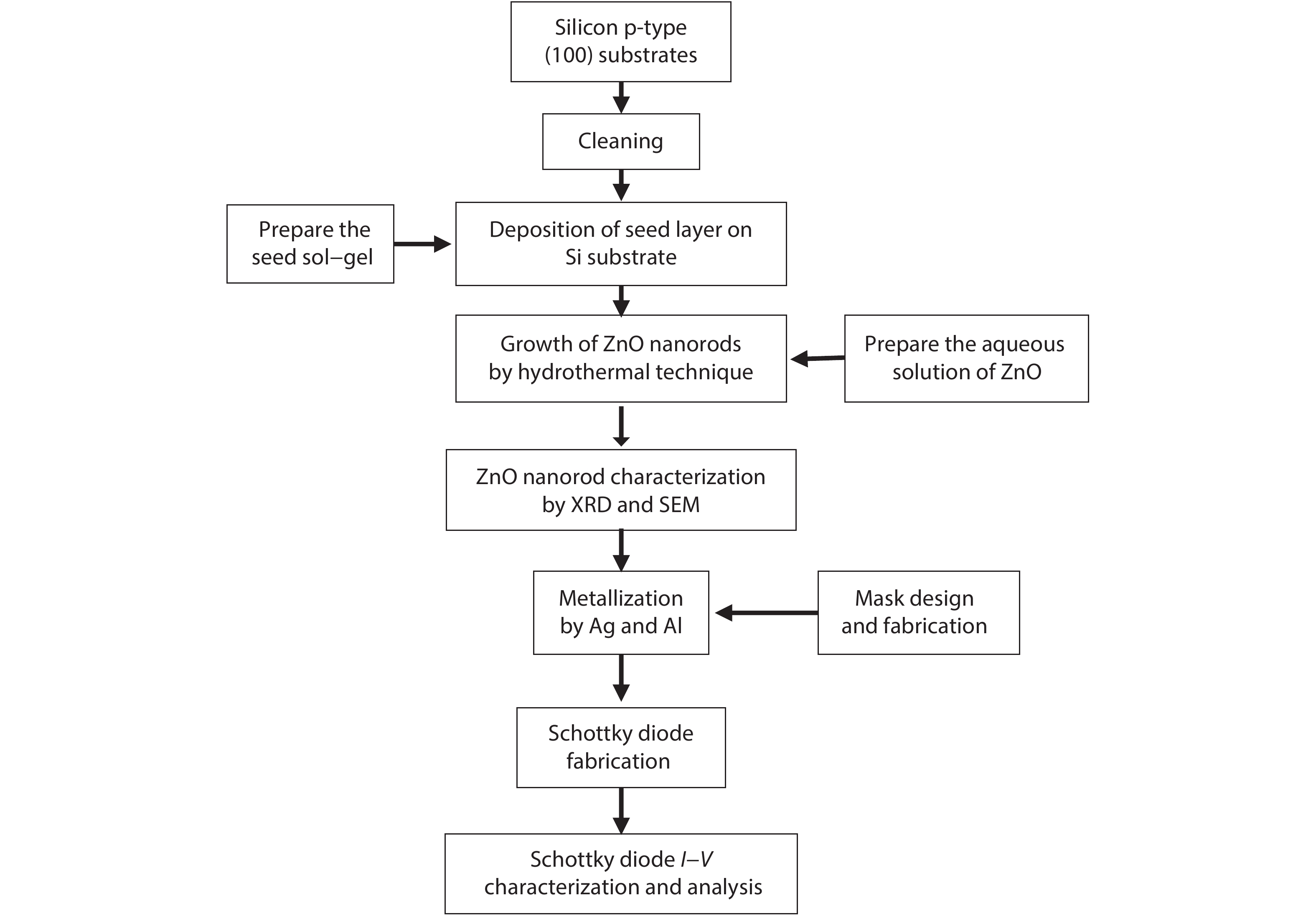
The crystalline structures of the resultant films were examined by XRD technique, with Cu Kα radiation (λ = 1.5406 Å) in 2θ ranging from 20° to 80°. The SEM was deployed to show the film surface topology. The I–V curves were carried out by a Keithley semiconductor characterization system (Keithley, SCS-4200) for applied voltage in the range of –3 to 3 V at room temperature. Fig. 1 shows the block diagram of the experimental work. Fig. 2 illustrates the schematic diagram of the experimental set-up, and the energy diagram of the Schottky Ag/ZnO contact.
![]()
Figure 1.The block diagram of the experimental work.
![]()
Figure 2.(Color online) (a) The schematic diagram of the experimental set-up. (b) The energy diagram of Schottky Ag/ZnO contact.
3. Result and discussions
Fig. 3 shows the SEM images of nanorod ZnO thin films deposited by the hydrothermal technique. Nanorod synthesis was by a simple solution-phase synthesis hydrothermal deposition method. The figure demonstrates vertically aligned nanorods combined in the central point. The ZnO combined nanorod growth produced flower-shaped ZnO nanostructures perpendicular to the substrate. The nanorod structure is a one-dimensional (1D) structure while the flower-like ZnO nanostructure is a three-dimensional (3D) structure. It is well-known that the 1D nanostructures have a very large surface area/volume ratio that raises the sensing performance in electronic devices. Still, there are some disadvantages to the 1D nanostructures regarding reliability and stability. The 3D nanostructures assembled by 1D nanostructure-based electronic sensing devices are more reliable and stable. In recent times, the assembly of 3D by 1D nanostructure units has been an attractive research area, however, little research has been done to study the effect of size controllable units on electronic device performances[
![]()
Figure 3.SEM of nanostructured ZnO thin films coated by hydrothermal technique. (a) Single nano-flower. (b) Multi nano-flowers.
The XRD patterns of the ZnO films grown on a silicon substrate by the hydrothermal method shown in Fig. 4 at 2θ from 20° to 80°. Fig. 4 shows the dominant peak appearing at (002). This intense peak indicates a c-axis orientation of the wurtzite structure. It is demonstrated that the crystals grow uniformly perpendicular to the substrate surface in good agreement with the SEM images. The other smaller peaks correspond to the (100), (101) and (102) planes of the hexagonal wurtzite ZnO thin film. This concludes that the hydrothermally grown ZnO film is a polycrystalline crystal structure with preferred (002) orientation. The FWHM of a hydrothermal film of dominant peak (002) at 34.3º is estimated to be 0.14º.
![]()
Figure 4.XRD pattern of ZnO thin films coated by hydrothermal technique.
The measured current–voltage plots of Ag/ZnO/Al planar diode at room ambient temperature presented a rectifying behavior, as shown in Fig. 5. The current across a Schottky barrier is described according to the thermionic emission expression[
![]()
Figure 5.
where A is the contact area of the fabricated planar diode that equals ~ 0.16 cm2, T is the temperature in Kelvin, q is the electron charge, A* is the effective Richardson constant (A* = 4πme*qk2/h3) of ZnO, which is about 32 A·cm–2·K–2 for me* = 0.27m0, V is the applied bias voltage, n is the ideality factor, ϕB is the barrier height and k is the Boltzmann constant.
To confirm the repeatability of the measured data, the I–V characteristics were carried out for many samples from different fabricated batches. The error bars in Fig. 5, demonstrate the variance in the current measurements for given applied voltage, represented by vertical lines. Based on the I–V curve shown in Fig. 5 and Eq. (4), the device performance parameters were estimated. From forward current for applied voltage larger than 3kT/q, the value of the saturation current (IS) was extracted by extrapolating the linear region of the ln I versus V plot to zero voltage. The value of the saturation current is found to be 1.2 × 10⁻⁶ A. The saturation current values were used to estimate the barrier height, ϕB = (kT/q)ln(AA*T2/IS). The computed barrier height values are 0.6908 eV. The rectification ratio at +3/–3 V is 23. The turn-on voltages are determined as 0.4 V. The device exhibits a very large ideality factor (n > > 2) which means that the measured forward current is much smaller than that computed theoretically by thermionic emission. This is due to high interface trap concentration[
4. Conclusion
This study presents ZnO thin film nanoflower compounds of nanorod structure were deposited by hydrothermal technique. The deposited ZnO films exhibit a c-axis with (002) orientation of the polycrystalline wurtzite structure. The resultant nanostructured ZnO thin film is utilized to fabricate the planar Ag/ZnO/Al Schottky junction. The electrical characteristic of the as fabricated diodes extracted from the I–V curves at room ambient temperature. The devices show rectifying behavior. The parameters such as the rectifying ratio, ideality factor, barrier height and reverse-bias leakage current are extracted from measured data. The study also revealed that the magnitude of the ideality factor was estimated to be significantly higher for all fabricated devices attributed to high interface trap concentrations. This work revealed that cost-effective undoped ZnO nanoflower film Schottky diodes can be deployed in sensors applications.
Acknowledgements
The authors would like to acknowledge the Microelectronics Lab, Electrical Engineering Department, College of Engineering, Mustansiriyah University, for technical assistance.
References
[1] J Y Tsao. Ultrawide-bandgap semiconductors: research opportunities and challenges. Adv Electron Mater, 4, 1(2018).
[2]
[3] L J Brillson, Y Lu. ZnO Schottky barriers and Ohmic contacts. J Appl Phys, 109, 8(2011).
[4] M A Borysiewicz, E Kamińska, M Myşliwiec et al. Fundamentals and practice of metal contacts to wide band gap semiconductor devices. Cryst Res Technol, 47, 261(2012).
[5] G M Ali. Interdigitated extended gate field effect transistor without reference electrode. J Electron Mater, 46, 713(2017).
[6] A B Yadav, A Pandey, S Jit. Pd Schottky contacts on sol –gel derived ZnO. IEEE Electron Device Lett, 35, 729(2014).
[7] D Somvanshi, S Jit. Analysis of temperature-dependent electrical characteristics of n-ZnO Nanowires (NWs)/p-Si heterojunction diodes. IEEE Trans Nanotechnol, 13, 62(2014).
[8] S Roy, S Das, C K Sarkar. Investigation of nanostructured Pd–Ag/n-ZnO thin film based Schottky junction for methane sensing. Int Nano Lett, 6, 199(2016).
[9]
[10] C A Mead. Surface barriers on ZnSe and ZnO. Phys Lett, 18, 218(1965).
[11] R C Neville, C A Mead. Surface barriers on zinc oxide. J Appl Phys, 41, 3795(1970).
[12] D Somvanshi, S Jit. Effects of Sn and Zn seed layers on the electrical characteristics of Pd/ZnO thin-film Schottky diodes grown on n-Si substrates. IEEE Electron Device Lett, 35, 945(2014).
[13] G M Ali, P Chakrabarti. Fabrication and characterization of thin film ZnO Schottky contacts based UV photodetectors: A comparative study. J Vac Sci Technol B, 30, 031206(2012).
[14] S Singh, P Chakrabarti. Comparison of the structural and optical properties of ZnO thin films deposited by three different methods for optoelectronic applications. Superlattices Microstruct, 64, 283(2013).
[15] D Somvanshi, S Jit. Effect of ZnO seed layer on the electrical characteristics of Pd/ZnO thin-film-based schottky contacts grown on n-Si substrates. IEEE Trans Nanotechnol, 13, 1138(2014).
[16] S Sharma, S Vyas, C Periasamy et al. Structural and optical characterization of ZnO thin films for optoelectronic device applications by RF sputtering technique. Superlattices Microstruct, 75, 378(2014).
[17] S Baruah, J Dutta. Hydrothermal growth of ZnO nanostructures. Sci Technol Adv Mater, 10, 013001(2009).
[18] H Zhang, W Chen, Y Li et al. 3D flower-like NiO hierarchical structures assembled with size-controllable 1D blocking units: Gas sensing performances towards. Acetylene, 6, 1(2018).
[19] A Gokarna, N R Pavaskar, S D Sathaye et al. Electroluminescence from heterojunctions of nanocrystalline CdS and ZnS with porous silicon. J Appl Phys, 92, 2118(2002).
[20] G M Ali, A D D Dwivedi, S Singh et al. Interface properties and junction behavior of Pd contact on ZnO thin film grown by vacuum deposition technique. Phys Status Solidi C, 7, 252(2010).


Set citation alerts for the article
Please enter your email address

© Copyright 2018-2021 | Chinese Laser Press. All Rights Reserved 沪ICP备15018463号-20