1Key Laboratory of Materials for High Power Laser, Shanghai Institute of Optics and Fine Mechanics, Chinese Academy of Sciences, Shanghai 201800, China
2University of Chinese Academy of Sciences, Beijing 100039, China
The inclusions in conventionally grown (DKDP) crystals are investigated. The inclusions are captured by a light-scattering technique. The sizes are determined by an optical microscope and a transmission electron microscope (TEM), and the compositions are analyzed by time of flight secondary ion mass spectrometry (TOF-SIMS) and an energy dispersive spectrometer (EDS). Two kinds of inclusions are observed in the DKDP crystals: a submicron-scale inclusion and a micron-scale inclusion. The typical submicron-scale inclusions contain growth solution, and their sizes range from tens to hundreds of nanometers, whereas the micron-scale inclusions contain growth solution and the metal element Na, and the sizes are tens of microns. The possible formation mechanisms of the inclusions are discussed, and the influence of the inclusions on laser-induced damage behaviors are analyzed and discussed.
(KDP) and (DKDP) crystals are important nonlinear crystals for frequency conversion and Pockels cells[1]. DKDP crystals have advantages in their nonlinear optical coefficients, and they can avoid the laser damage induced by stimulated Raman scattering, which exists in the KDP crystal, which was used as a frequency tripler and converter[2]. A serious problem for the DKDP crystal has been the low laser-induced damage threshold of the third harmonic generation (THG) laser. The prevailing viewpoint was that the precursor absorbed the energy efficiently and gave rise to laser damage. Bulk defects might be responsible for the damage initiations, such as impurities[3,4], inclusions, interstitial atoms, and vacancies. An important bulk defect in KDP/DKDP crystal was inclusions, and a lot of work has been done to study it. Different formation mechanisms of inclusions have been discussed. Janssen considered that the formation of liquid inclusions was a result of the depletion in the stable eddies formed at the rear faces[5]. Van Enckevort thought that the liquid inclusions were induced by the temperature fluctuation of the growth solution[6,7]. Smolski found that inclusions were not directly formed by dislocations, and might caused by foreign particles[8]. Zaitseva believed that inclusions were preceded by visible intervicinal boundaries between the edges, and visible intervicinal boundaries between the edges and dislocation slopes[9]. Sun interpreted the formation of inclusions as an overhang of macrosteps induced by impurities with large dimensions[10].
Previous works found that bulk defects might have a connection with the optical properties of the DKDP crystal[11,12]. In this Letter, inclusions in conventionally grown DKDP crystals are studied. Possible formation mechanisms of the inclusions are discussed. The formation mechanism of the inclusions was not unique.
The DKDP boule was grown by the conventional growth method. A pure reagent ( raw material) and 70% deuterated extra-pure water were used for the growth solution preparation. The raw material had an effect on the properties of the crystal[13], so the purity of the raw material was analyzed by inductively coupled plasma mass spectrometry (ICP-MS), the detection limit of which was 0.1 ppb. The mass contents of the main impurities are shown in Table 1. The content of Na was less than 4.5 ppm, which was much higher than the others. The DKDP boule was cut into plates in tripling-cut[14]. The DKDP witnesses were well polished by single-point diamond finishing, and cleaned with ethanol.
Sign up for Chinese Optics Letters TOC. Get the latest issue of Chinese Optics Letters delivered right to you!Sign up now
Element
Fe
Cr
Al
Ba
Ca
Zn
Mn
Na
Pb
Mg
Cu
Cd
ICP-MS (ppm)
<0.05
<0.05
<0.05
<0.05
<0.18
<0.05
<0.05
<4.5
<0.05
<0.05
<0.05
<0.05
Table 1. The Mass Contents of Main Impurity Elements in the KH2PO4 Raw Material
A light-scattering technique was used to detect the bulk defects in the DKDP crystal, the system of which was described in Ref. [12]. A continuous 532 nm laser with a Gaussian spatial profile illuminated the bulk site at a power of 1.3 W. The effective area of the spot on the sample was . The images of the scattering defects were captured at the direction orthogonal to the irradiation path.
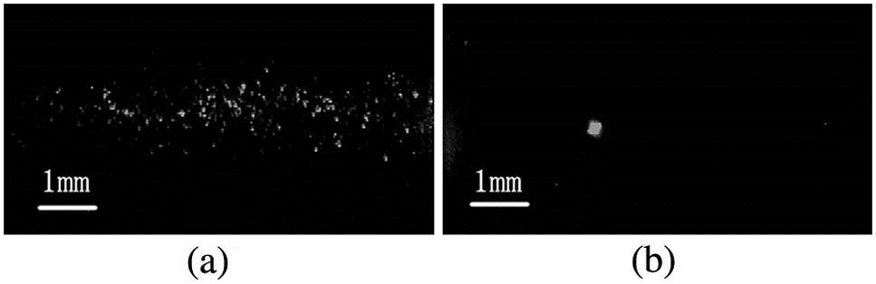
The scattering defects in the DKDP crystal are shown in Fig. 1. Two kinds of unique defects were found. One was the scattering defect with a high density shown in Fig. 1(a); another was the sparsely distributed scattering defect shown in Fig. 1(b). The two kinds of defects were named from the sizes described in the next paragraph. The former was named the submicron-scale defect, and the second was named the micron-scale defect.
Figure 1.(a) Submicron-scale and (b) micron-scale defects in DKDP crystal detected by the light-scattering technique.
In order to observe the morphologies of these scattering defects, different measurements were employed according to their properties. The size of submicron-scale was small, so transmission electron microscope (TEM) HT7700 was employed to get the morphology. A slice of the DKDP crystal that was not close to the surface was cut with a thickness of around 1 μm by an ultra-microtome, and fabricated to 200 nm by an ion beam thinner. Then, it was observed by the TEM at the working voltage of 100 kV. At the same time, energy dispersive spectrometer (EDS) was used to analyze the composition of the submicron-scale inclusion within the visual field of the TEM.
Figure 2 shows the morphology of the submicron-scale defect in the DKDP crystal observed by the TEM. The observed submicron-scale defect has a ball-like shape, and the size ranges from tens to hundreds of nanometers. The submicron-scale defect was brighter than the DKDP crystal. The image contrast of the TEM depended on the transmittance of the electrons through the slice, which were affected by the thickness and composition of the DKDP crystal. Because the thickness of the observed area was constant, it was indicated that the composition of the submicron-scale defect was different from the DKDP crystal. The result of the EDS analysis is shown in Fig. 3. As the slice was cut inside the DKDP crystal, the pollution from the polishing was ignored. In the experiment, the slice was fixed by a copper ring, and the test platform was polluted by Al and Si. So the elements of Cu, Al, and Si detected by the EDS were not the impurities of the submicron-scale defect. No impurity was detected in submicron-scale defect besides the pollution. We supposed the submicron-scale defect to be growth solution or air, the composition of which was also different from the DKDP crystal. However, the submicron-scale defect could be eliminated by laser conditioning[12]; thus, it could not be air. Then, it was suggested that the material in the submicron-scale defect was liquid, and that the ball-shaped defect was a liquid inclusion[15]. The submicron-scale defect was a submicron-scale inclusion.
Figure 2.Morphology of submicron-scale inclusion in the DKDP crystal observed by the TEM.
Two possible formation mechanisms were suggested. First, thermodynamic inhomogeneity could be the reason leading to the submicron-scale inclusion[16]. Thermodynamic data was an important factor for crystal grown from the solution. It affected the metastable zone, growth rate, and nucleation. It was difficult to control the cooling and stirring precisely, so the thermodynamic data of the growth solution was likely to be locally inhomogeneous. This would lead to a submicron-scale inclusion. Second, because dislocation was found around the submicron-scale inclusion in Fig. 2(a), the viewpoint raised by Zaitseva[17] that the inclusion was preceded by an intervicinal boundary between the edge and dislocation slope could be a reasonable explanation for the submicron-scale inclusion observed.
On the other hand, the micron-scale defect had a relatively large size and might be observed by the optical microscope. However, the defect was embedded in the crystal at the depth of 3 mm and cannot be directly observed due to the limited working distance of the microscope. The DKDP crystal was etched in 60% distilled water and a 40% ethanol solution until the micron-scale inclusion was very close to the surface. Then, the morphology was observed by the optical microscope PM6000 at a magnification of 250 times. Figure 4 shows the morphology of the micron-scale defect. The micron-scale defect consisted of two parts: the core and the surrounding material. The interface between this defect and the DKDP crystal was obvious. By adjusting the focal length of the optical microscope, we observed the three-dimensional structure of the micron-scale defect. The ball-like defect could be a liquid inclusion, the size of which was tens of microns, according to Ref. [18].
Figure 4.Morphology of the micron-scale inclusion in the DKDP crystal observed by the microscope PM6000.
Because impurities were detected in the raw material, as shown in Table 1, the composition of the micron-scale inclusion was analyzed. The distributions of the impurities in Table 1 and N, S, C, Cl, Si were analyzed. As the micron-scale inclusion had a three-dimensional structure, time of flight secondary ion mass spectrometry (TOF-SIMS, TOF.SIMS 5-200) was used to analyze the composition of the micron-scale inclusion. All the results of the TOF-SIMS were non-quantitative. The analyzed field was . Because the sample was etched a lot and the micron-scale inclusion was still embedded in the DKDP crystal, the pollution from the single-point diamond was ignored. A Na gathering was observed (Fig. 5), while the other element was evenly distributed in the analyzed field. The size of the Na-rich region in the planar direction was tens of microns, which was the same as the micron-scale inclusion shown in Fig. 4. The size in the depth direction was around 2 μm. Thus, it was suggested that the micron-scale inclusion was a flat ellipsoid.
Figure 5.The result of the TOF-SIMS analysis. (a) The distribution of in the DKDP crystal at the depth of 1.5 μm. (b) The three-dimensional distribution of in the detected area.
The content of Na in the raw material was about 4.5 ppm, so it was speculated that the micron-scale inclusion was induced by an impurity gathering. The DKDP crystal grew on vicinal hillocks formed by dislocation. During the growth of the perfect DKDP crystal, the elementary steps in the step trains were parallel. When was doped into the growth solution, these impurity atoms took the place of the DKDP atoms. Then, the step trains were distorted by the impurity atoms, and the steps behind these atoms were slowed down. Although a few elementary steps were slowed, the macrosteps moved on, and some growth solution was wrapped up in the DKDP crystal. In this way, a micron-scale inclusion was formed. The normal growth rate of a crystal face, , was given[19]where is the slope of the dislocation hillock, and is the tangential speed of the elementary steps. Because [1], the normal rate was much less than . The exposure time in the growth solution for atoms in different growth directions was different for each one. The longer the impurities were exposed in the growth solution, the more the steps were distorted[20]. So the distorted steps in different directions were discrepant. Therefore, the micron-scale inclusion grew into a flat ellipsoid.
To investigate the influence of the inclusions on laser-induced damage behaviors, a damage test experiment of the DKDP crystal was performed at the bench described in Ref. [12] with a pulsed Nd:YAG laser operating at 10 Hz, the duration of which was 12 ns. A ramp (R-on-1) test was employed to analyze the laser damage resistance, and 50 test points were chosen. Figure 6 shows the damage probability curves (1064 nm, 12 ns) of the DKDP crystals with/without micron-scale inclusion. The laser damage threshold of the DKDP crystal with the micron-scale inclusion was , which was far below , the laser damage threshold of the DKDP crystal without the micron-scale inclusion. To understand this drop in the laser damage threshold, the scattering images before and after the irradiation were studied. Figure 7 shows the pinpoint damages in the DKDP crystal with the micron-scale inclusion at . Figure 7(a) is the scattering image before irradiation, and Fig. 7(b) is the image of the pinpoint damage after irradiation. When irradiated by a 1064 nm laser at , damages initiated from the micron-scale inclusions. The micron-scale inclusion induced laser damage at a low fluence.
Figure 6.R-on-1 laser damage probability curve of the DKDP samples.
Two possible mechanisms of micron-scale inclusion absorption were suggested. First, the doped growth solution in the micron-scale inclusion was absorptive. A gathering was detected in the micron-scale inclusion, and the doped growth solution was conductive. The absorption coefficient of conductive solution was concentration-related[21]: where is the absorption coefficient, is the constant related to the solute, and is the concentration of the doped growth solution. The absorption coefficient of the growth solution in the micron-scale inclusion was much higher than the DKDP crystal. Second, the hydrogen or deuterium (H/D) defect at the interface between the micron-scale inclusion and the DKDP crystal could generate absorption[22]. The structure of the DKDP crystal was made of units linked by an O-H(D)-O network. But the growth step at the micron-scale inclusion was distorted, and the crystallization was incomplete. The O-H(D)-O network was destroyed, and H/D defects formed at the interface, such as charged the H/D interval and the H/D vacancy. These defects played an important role in photon absorption.
A model simulating transient optical properties during the laser damage in the bulk of KDP/DKDP crystals was presented by Demos et al.[23]. The model suggested that the precursors with a high density of defects and large size would initiate damage at a low fluence. The micron-scale inclusion observed in this paper might induce laser damage at a low fluence. When irradiated by a laser beam, the micron-scale inclusion was heated and the secondary defect was formed. Because the laser intensity remained high for a sufficient time to heat the micron-scale inclusion to a certain temperature, the conduction band electron population reached a high density. At this point, the conduction band electron multiplication process and the plasma formation process expended the remaining energy of the pulse, and laser damage was induced.
In conclusion, two types of inclusions in DKDP crystals grown by the conventional growth method are observed: a submicron-scale inclusion and a micron-scale inclusion. The submicron-scale inclusion might be caused by thermal inhomogeneity or the intervicinal boundary between the edge and dislocation slope. The micron-scale inclusion is indicated to be induced by impurities. Laser damage initiated from the micron-scale inclusion is observed by the ramp test. The doped growth solution or H/D defects might be responsible for the laser absorption. The damage initiated from the micron-scale inclusion is consistent with Ref. [23].