• Journal of Semiconductors
  • Vol. 42, Issue 3, 032402 (2021)
Xiangyu Li1、2, Pengyuan Jiao1、3, and Chaoqun Yang1、3
Author Affiliations
  • 1Institute of Microelectronics, Tsinghua University, Beijing 100084, China
  • 2Beijing National Research Center for Information Science and Technology, Beijing 100084, China
  • 3School of Applied Science, Beijing Information Science and Technology University, Beijing 100192, China
  • show less
    DOI: 10.1088/1674-4926/42/3/032402 Cite this Article
    Xiangyu Li, Pengyuan Jiao, Chaoqun Yang. Side-channel attack-resistant AES S-box with hidden subfield inversion and glitch-free masking[J]. Journal of Semiconductors, 2021, 42(3): 032402 Copy Citation Text show less

    Abstract

    A side-channel attack (SCA)-resistant AES S-box implementation is proposed, which is an improvement from the power-aware hiding (PAH) S-box but with higher security and a smaller area. We use the composite field approach and apply the PAH method to the inversion in the nonlinear kernel and a masking method to the other parts. In addition, a delay-matched enable control technique is used to suppress glitches in the masked parts. The evaluation results show that its area is contracted to 63.3% of the full PAH S-box, and its power-delay product is much lower than that of the masking implementation. The leakage assessment using simulation power traces concludes that it has no detectable leakage under t-test and that it at least can thwart the moment-correlation analysis using 665 000 noiseless traces.

    1. Introduction

    Side-channel attack (SCA) resistance is an important issue in the design of cryptographic integrated circuits in many applications, including the internet of things (IoT) nodes[1]. Accordingly, SCA countermeasures must be employed in most IoT devices for security and privacy. However, IoT devices are usually lightweight systems. Therefore, the countermeasures for IoT devices must be secure, energy-efficient and low-cost at the same time.

    The advanced encryption standard (AES) is widely used in IoT systems[2] and the key point for addressing these challenges for AES is usually to realize a low-power, low-cost, and secure S-box.

    The state-of-the-art uses key updating[3], which is a kind of leakage resilience method. However, although it is low-overhead, it requires both sides of communication to use the same key update mechanism, which is not always realizable. The masking method randomizes intermediates of a calculation making use of random masks, but is complex when it is applied to nonlinear operations. Even though it can achieve a small area (e.g. the threshold implementation method[4-6]), the energy efficiency is still relatively low. The threshold implementations of AES S-box usually take tens of cycles for one computation. Concerning the hiding methods, most of the equalization methods[7] or the noising methods[8] must consume extra energy as the compensation or noise component. Random voltage or clock dithering[9] has less overhead but its effectiveness will be decreased when enhanced alignment technique (e.g. elastic alignment[10]) is used. Ref. [11] does not illustrate any considerations about the internal power difference of the dual-rail flush logic (DRFL) gates and early propagation issues. Moreover, like most of dual-rail DPA-resistant logic styles, it needs to develop a new library of full-custom gates. The power-aware hiding (PAH) method[12, 13] is a new kind of power equalization technique that minimizes the compensation power and addresses the early propagation issue. Moreover, it supports semi-custom design flow. However, its area is too large area to be used in the IoT applications, which are sensitive to cost (e.g. RFID tags).

    We proposed a novel AES S-box implementation method in Ref. [14], which shrinks the scope of the PAH method in the design to dramatically decrease the area of circuit in addition to the mismatch in PAH block. As an expansion of this conference paper, in addition to a more detailed discussion and evaluation of the PAH part, this paper presents a glitch-free implementation of the masked part in the proposed structure that has enhanced the security of the whole design. On the whole, this new solution results in a higher level of security with a low area and a high energy efficiency.

    2. Related countermeasures

    2.1. Full-masking structure

    The scheme developed by Canright[15] is a classic tower-field masking architecture. The AES S-box consists of the following two substeps: inversion in GF(28) and an affine transformation. The inversion in GF(28) can be calculated in the subfield GF(24), which in turn involves operations in GF(22), to minimize the area. The masked inversion calculation in the Canright approach can be depicted as in Eqs. (1)–(5), where is the input data masked (XORed) by a random byte (mask), M, i.e., ; and subscript 1 or 0 attached with the symbols indicates their high or low 4 bits, respectively. The symbol Inv*() in Eq. (2) denotes the masked inversion operation in GF(24). This generates masked by M1, denoted by . Q is another 4-bit mask independent of M. In addition, a 2-bit mask (r) joins the calculation over GF(22). The final output is the masked output and its mask M. This approach requires all intermediates to be masked and is termed the “full-masking implementation.”

     (1)

     (2)

     (3)

     (4)

     (5)

    2.2. Power-aware hiding technique

    The power-aware hiding technique implements an N-bit substitution function as a lookup table (LUT). The function output is expanded by a flag bit and N/2 compensation bits. The LUT is generated according to the following rules: when the Hamming weight (HW) of the original result is greater than N/2, the resulting word in the table is its inverted value, and the flag bit is 1; otherwise, the result word in the table is the original value, and the flag bit is 0. The compensation bits have a proper number of bits being ones; thus, the HW of the whole output word is N/2. The method presented in Refs. [12, 13] is to implement the entire design in the way of PAH as a whole function (which will be termed the “full-PAH” implementation in this paper). This implementation has advantages in terms of power-delay product (PDP) and performance, whereas its area overhead is too expensive for cost-sensitive applications. More importantly, it has many 4-input AND gates and therefore its stack-effect is relatively severe, which is a main source of mismatch in the circuit. Additionally, a larger block usually has larger clock skews between the gates. The clock skews can cause data-related difference in terms of timing, and afterwards power, in dynamic logics. For these two reasons, the larger scale PAH array has a more significant power difference.

    3. Masked AES S-box with PAH GF(24) inverter

    3.1. PAH-masking mixed architecture

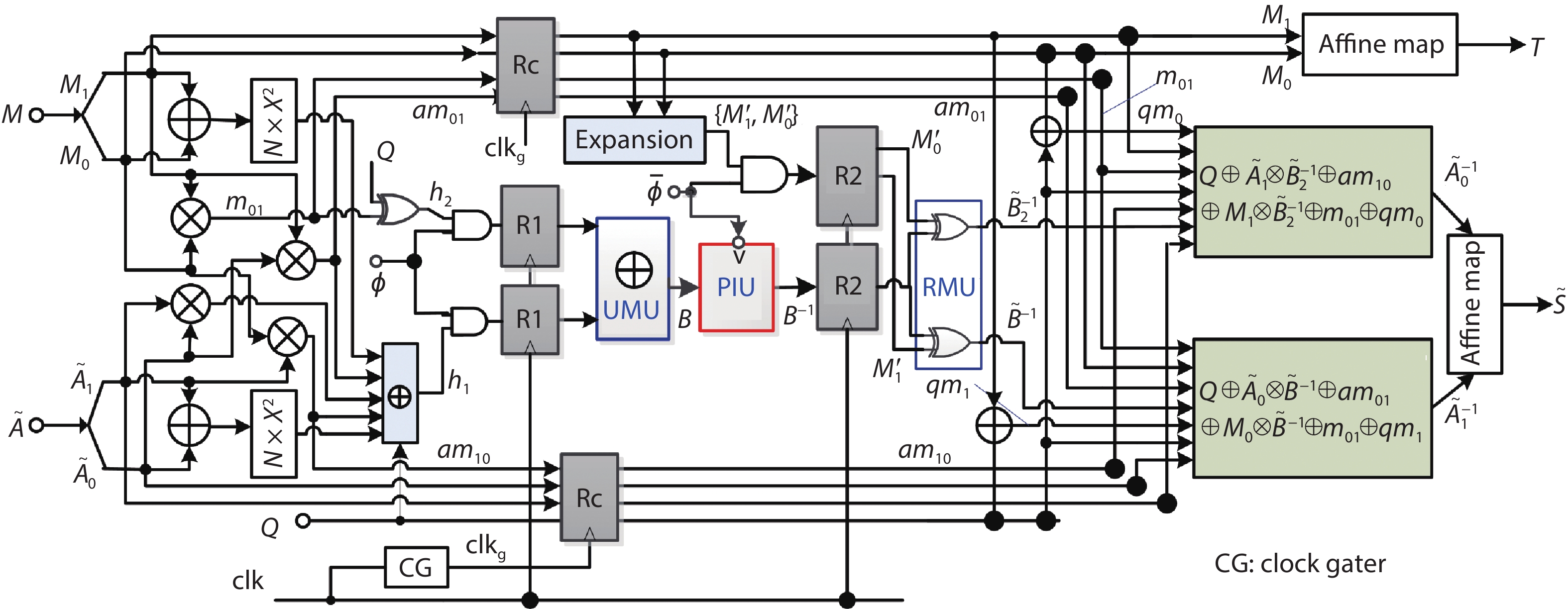
    In the proposed architecture, the inverse calculation in GF(24) is implemented by means of PAH rather than the masked subfield GF(22) calculation. The other operations are still in the masking approach. Hence, the proposed implementation is given by Eqs. (4)–(10), where Invh() represents the inversion in GF(24) implemented in the PAH manner. The input of the PAH inversion unit (PIU) should be unmasked before entering the PIU. The output of PIU ( ) is also remasked immediately after output; see Eqs. (9) and (10).

     (6)

     (7)

     (8)

     (9)

     (10)

    PIU operates in two phases: precharge and evaluation (see Section 3.2). Therefore, the proposed S-box module is implemented as a two-phase pipeline. As shown in Fig. 1, there are two register stages, R1 and R2, which divide the datapath into three stages. Fig. 2 gives its timing diagram. The phase of the pipeline is controlled by a pair of inverse signals switching at every rising clock edge: and . The first stage calculates h1 and h2. The second stage completes the inversion. In addition to PIU, there is an unmasking unit (UMU) that adds h1 and h2 together to unmask B. The masks of and are also prepared in this stage. The third stage calculates the final output ( ) and its mask (T). In this stage, is masked by M1 and M0, respectively, at a remasking unit (denoted by RMU) and becomes and . The rest logic of the third stage functions as Eqs. (4) and (5), in addition to the basis change and the affine transformation of and its mask. These stages output fixed values in their respective precharge phase. The variables that appear in both the first and the third stage, such as (denoted by am10), (denoted by am01), (denoted by m01), and so on, are latched by a group of registers named Rc, which is updated only once for each computation.

    (Color online) PAH-masking mixed S-box structure (modified from Ref. [14]).

    Figure 1.(Color online) PAH-masking mixed S-box structure (modified from Ref. [14]).

    (Color online) PAH-masking mixed S-box timing diagram (modified from Ref. [14]).

    Figure 2.(Color online) PAH-masking mixed S-box timing diagram (modified from Ref. [14]).

    3.2. PAH GF(24) inversion unit

    The circuit of the PIU is a 16-entry LUT implemented as a domino logic array. The signal is its clock. According to the principle of PAH[12], its outputs include a 4-bit result word, a flag bit, and two compensation bits. The logic of each output bit is implemented as a sum of products. The numbers of products of all bits of the result word and also the flag bit are 5. The numbers of products of the two compensation bits are 3 and 4, respectively. As shown in Fig. 3, the whole PAH unit contains an AND-plane, which produces all 16 product terms, and an OR-plane, which is composed of seven dynamic OR gates. The PIU input is encoded in 1-of-4 code; thus, the input data are represented by two groups of wires. Each input of an AND gate comes from one of the two groups and corresponds to one possible pattern of its group. Hence, the number of input transitions is kept constant (equals to 2). There are always one and only one product signal transition, and two and only two output transitions in the array for any input pattern. Some additional transistors used to precharge the internal nodes in the ANG gates for the purpose of restraining charge sharing and making their initial states before evaluation consistent for different input pattern. Using domino logic, the OR gates avoid series connection of five PMOS transistors. In addition, the static power consumption is closed to the static complementary CMOS logic. Additionally, PIU's operation is naturally divided into precharge and evaluation phases, which is necessary for making switching activity constant. Such a regular array can automatically be implemented by a compiler, as presented by Ref. [12]. The noise and mismatch of each gate are predictable. Hence, the problems about robustness and design effort brought by domino logic are not challenges in this case. For a new process, we only need to re-design a small number of basic layout cells, whose design difficulty is much lower than those special power-balanced logic style gates.

    (Color online) PAH inversion in GF(24) unit. (a) Circuit[14]. (b) Layout (62 × 56 μm2).

    Figure 3.(Color online) PAH inversion in GF(24) unit. (a) Circuit[14]. (b) Layout (62 × 56 μm2).

    To control for the difference of internal power, all gates in the same plane have identical fan-in, fan-out and size. For the OR gates, of which actual fan-ins are fewer than five, the unused input pins are connected to ground (dotted line transistors in Fig. 3(a)). In addition, the flip-flops of R2 employ the same kind of cells, so that the power consumption of the output data transition is constant.

    Consequently, PIU has only 16 2-input AND gates and 7 5-input OR gates, while the full-PAH S-box has 256 4-input AND gates and 13 93-input OR gates[12]. A smaller number of entries not only saves the area but also benefits clock skew minimization because the overall routing length of the clock network is shorter. The clock skew will cause a mismatch of the evaluation or precharge time point of the gates, and hence will result in difference on power traces. In addition, the fan-in of the AND gates in PIU is smaller than that of the full-PAH S-box, and thus the mismatch due to stack-effect is much smaller. These advantages can decrease the power difference of the PAH array. Another benefit brought by the smaller fan-in of the AND gates is a lower minimum operating supply voltage. A low supply voltage is an important technique that can be used in energy-efficient circuits. The lowest supply voltage of this circuit achieves 0.4 V, which is a near-threshold value, which is the typical high energy-efficiency operating supply voltage range.

    3.3. Un/Remasking circuits

    Unmasking and remasking must be implemented with power-balanced circuits because unmasked intermediates appear in them. Therefore, the inputs of UMU, h1 and h2, are converted into 1-of-4 code in advance to facilitate power equalization because the XOR logic of the 1-of-4 data has a symmetric structure and is glitch-free. In RMU, are masked with M1 and M0 in parallel. This is completed by the following two steps. First, (in the 2-of-7 PAH code) are XOR-ed with and , respectively, both of which are 7-bit masks derived from M1 and M0, respectively, by introducing three additional random bits. Second, the masked data are decoded into 4-bit normal binary data. This two-stage structure provides uniform fan-outs for all 7 flip-flops of .

    To power-balance the RMU circuit, the XOR gates in it adopt the same cell. However, the XOR cells in the standard cell library are not satisfied. Their structure is shown in Fig. 4(a). The loads of the two input pins are different. Therefore, the transition power consumption of the gate will be different when different input pin switches are used. For the sake of eliminating this power difference, a kind of symmetric XOR gate is used instead; as shown in Fig. 4(b). In the symmetric gate, two identical XOR gates (whose input pins are cross connected) are combined in parallel. Thus, the capacitance at the two inputs is symmetric.

    Modification of XOR gates in RMU.

    Figure 4.Modification of XOR gates in RMU.

    3.4. Glitch elimination in the masking domain

    Glitches in the combinational logic pose a non-ignorable threat to masked implementations, especially to the XOR-chain structures[16]. Therefore, the terms in Eqs. (4)–(6) must be added individually in a proper sequence[15]; thus, each one forms an XOR-chain. To suppress glitches of RMU and UMU, their inputs are synchronized by registers; as shown in Fig. 1. Meanwhile, an enable signal is introduced into the XOR-chains to eliminate the dangerous glitches in them.

    The glitch-free structure of the chain that calculates is shown in Fig. 5. Its XOR-chain (including the XOR in the multiplier, which is not drawn) is composed of six synchronized-XOR (Syn-XOR) gates and an “enable chain” (colored in grey). A Syn-XOR gate has an additional enable pin. The original input signal can affect the XOR gate only when enable =1. The enable chain is a duplication of the critical path that stems from the signal and is used to match the path delay. It is shared by all slices of the block. When is activated, the enable signal will be launched and it propagates along the enable chain to activate the Syn-XOR gates when their critical signals have arrived. Hence, at most, one transition can occur at each XOR gate during one evaluation. The enable signals are reset by the fall of . The AND gates driving the enable pins are used to speed up this reset procedure to avoid the early arriving signals, such as am01, causing transitions when enable has not fallen in the reset procedure.

    Structure of calculation logic with enable chain.

    Figure 5.Structure of calculation logic with enable chain.

    4. Implementation results

    The proposed S-box has been implemented in a 180 nm technology. PIU (including circuit and layout), which was generated with a macro compiler. The RTL description of the entire S-box was synthesized at first to obtain a standard-cell-based initial gate-level netlist. Next, the obtained netlist was modified manually, as follows: (1) the XOR-chains were replaced with the glitch-free structure shown in Fig. 5, where the critical path in the initial netlist was cloned as the delay matching logic; (2) the cells of UMU and RMU were modified so that all bit slices are identical. Then, after validation, the modified gate-level netlist was transformed into a SPICE netlist, in which the GF(24) inverter made of standard cells was replaced with the transistor-level PIU netlist. Finally, the transistor-level design was verified, evaluated, and analyzed through SPICE simulation. For comparison, the unprotected Canright S-box[17], the full-masking and the full-PAH[13] designs are also implemented in the same technology.

    Concerning the security of the implemented S-box, the maximum of the proposed designs and also the full-masking, the full-PAH, and the unprotected S-box were obtained by a 10000-sample Nonspecific t-test[18], in which two datasets, one random, another fixed data, were used as the input of the S-box to obtain power traces. The power traces of all the circuits were collected through simulation in SPICE, with the sampling rate of 10 GSa/s. A t-test was then performed on the traces of the two datasets. The detail results of t-test of the designs are shown in Fig. 6, where the red lines indicate the general threshold to reject the null hypothesis ( [18]). The proposed S-box is the only one that reveals no significant difference. Hence, the leakage of PIU has proven to be less than that of the 256-entry PAH module.

    (Color online) Nonspecific t-test results (with 10 000 traces). (a) Unprotected. (b) Full-masking. (c) Full-PAH. (d) Proposed.

    Figure 6.(Color online) Nonspecific t-test results (with 10 000 traces). (a) Unprotected. (b) Full-masking. (c) Full-PAH. (d) Proposed.

    The maximum values of different S-boxes are compared in Table 1. Besides the designs in Fig. 6, we also include the leakage metric of the random fast voltage dithering (RFVD) method[9] and the proposed S-box but with a normal masking part (with glitches). The proposed design wins out. The security improvement due to the glitch-free design is also illustrated. It also shows that even with glitch leakage, the solution based on PIU and masking is still more secure than the full-PAH solution.

    Table Infomation Is Not Enable

    Additionally, the measurements to disclosure (MTD) values of this work and the unprotected S-box were measured by the first order moments-correlating profiled DPA (MCP-DPA)[19], in which the mean traces of different data were estimated through a random dataset and then the correlation power analysis based on Pearson's correlation of samples with the profiled mean values was performed on another random dataset. The result of the MCP-DPA on the proposed implementation using 665 000 traces is shown in Fig. 7. The correct key has not been revealed using these traces, so its MTD is greater than 665 000. Note that these traces have no noise because they are collected by simulation. For a real chip, the MTD value will be much larger.

    (Color online) MCP-DPA attack result (332 500 traces for profiling and 332 500 traces for correlation).

    Figure 7.(Color online) MCP-DPA attack result (332 500 traces for profiling and 332 500 traces for correlation).

    With respect to the performance and cost of the proposed method, Table 2 compares the delay (the latency of lookup), energy per-operation, and the area of different DPA-resistant AES S-boxes. With respect to the latency data of the proposed design, it is the sum of the delays of the three stages of logics in addition to the overhead time (setup and propagation time) of the registers[14]. The highest clock frequency of it is 333 MHz. The following points can be observed: with the proposed method: the area is shrunk to 61.2% of the full-PAH area, the energy is approximately 17.6% of the improved masking solution proposed in Ref. [20]. The energy efficiency and area of the proposed S-box are, respectively, worse than the full-PAH one and the masking one. Compared with the other candidates, this work provides a more balanced tradeoff between the cost and energy efficiency. Meanwhile, it achieves a higher level of security compared with both of them.

    Table Infomation Is Not Enable

    5. Conclusion

    Applying the PAH technique to the inversion in GF(24) in a masked tower-field implementation of AES S-box can realize higher security, and a good tradeoff between energy efficiency and cost. Based on the wave pipeline structure, an enable-based glitch-eliminating method can be used to further improve the security of the masked part. Implemented in a 180 nm process, it achieves 26.87 pJ/operation energy, 2365 gates equivalent, and no detectable leakage. It provides a high-security and overhead-balanced selection for AES S-box implementation. In the future, we will study its performance under a low voltage to explore energy-efficiency optimization through voltage scaling.

    Acknowledgements

    This work was supported by the National Science and Technology Major Project of China (2017ZX01030301).

    References

    [1] D Dinu, I Kizhvatov. EM analysis in the IoT context: Lessons learned from an attack on thread. IACR Trans Cryptogr Hardw Embed Syst, 73(2018).

    [2] K L Tsai, Y L Huang, F Y Leu et al. AES-128 based secure low power communication for LoRaWAN IoT environments. IEEE Access, 6, 45325(2018).

    [3] M Taha, P Schaumont. Key updating for leakage resiliency with application to AES modes of operation. IEEE Trans Inform Forensic Secur, 10, 519(2015).

    [4] A Moradi, A Poschmann, S Ling et al. Pushing the limits: A very compact and a threshold implementation of AES. Adv Cryptol - EUROCRYPT 2011, 69(2011).

    [5] S Gao, A Roy, E Oswald. Constructing TI-friendly substitution boxes using shift-invariant permutations. Cryptographers Track RSA Conference, 433(2019).

    [6] E Boss, V Grosso, T Güneysu et al. Strong 8-bit Sboxes with efficient masking in hardware extended version. J Cryptogr Eng, 7, 149(2017).

    [7] F Burns, A Bystrov, A Koelmans et al. Security evaluation of balanced 1-of-n circuits. IEEE Trans VLSI Syst, 19, 2135(2011).

    [8] P C Liu, H C Chang, C Y Lee. A low overhead DPA countermeasure circuit based on ring oscillators. IEEE Trans Circuits Syst II, 57, 546(2010).

    [9] A Singh, M Kar, S Mathew et al. Improved power side channel attack resistance of a 128-bit AES engine with random fast voltage dithering. European Solid-State Device Research Conference, 51(2017).

    [10] J G J van Woudenberg, M F Witteman, B Bakker. Improving differential power analysis by elastic alignment. Cryptographers Track RSA Conference, 104(2011).

    [11] S Lu, Z Zhang, M C Papaefthymiou. A 1.25 pJ/bit 0.048 mm2 AES core with DPA resistance for IoT devices. IEEE Asian Solid-State Circuits Conference, 65(2017).

    [12] J S Ma, M Y Wang, X Y Li. Power-aware hiding method for S-box protection. Electron Lett, 50, 1604(2014).

    [13] X Y Li, C Q Yang, J S Ma et al. Energy-efficient side-channel attack countermeasure with awareness and hybrid configuration based on it. IEEE Trans VLSI Syst, 25, 3355(2017).

    [14] C Q Yang, X Y Li, S J. Yin. Low-cost energy-efficient side-channel attacks resistant AES S-box with power-aware hiding inverter in GF(24). International Conference on Trust, Security and Privacy in Computing and Communications, 1526(2018).

    [15]

    [16] S Nikova, V Rijmen, M Schläffer. Secure hardware implementation of nonlinear functions in the presence of glitches. J Cryptol, 24, 292(2011).

    [17] D Canright. A very compact S-box for AES. Conference on Cryptographic Hardware and Embedded Systems, 441(2005).

    [18] T Schneider, A Moradi. Leakage assessment methodology. Conference on Cryptographic Hardware and Embedded Systems, 495(2015).

    [19]

    [20] J L Zeng, Y Wang, C Xu et al. Improvement on masked S-box hardware implementation. IEEE International Conference on Innovations in Information Technology, 113(2012).

    Xiangyu Li, Pengyuan Jiao, Chaoqun Yang. Side-channel attack-resistant AES S-box with hidden subfield inversion and glitch-free masking[J]. Journal of Semiconductors, 2021, 42(3): 032402
    Download Citation