
Xueqing Cui, Ranran Xie, Hongliang Liu, Yuechen Jia, Feng Chen. Lithium niobate metasurfaces: preparation and photonics applications[J]. Opto-Electronic Engineering, 2022, 49(10): 220093
- Opto-Electronic Engineering
- Vol. 49, Issue 10, 220093 (2022)
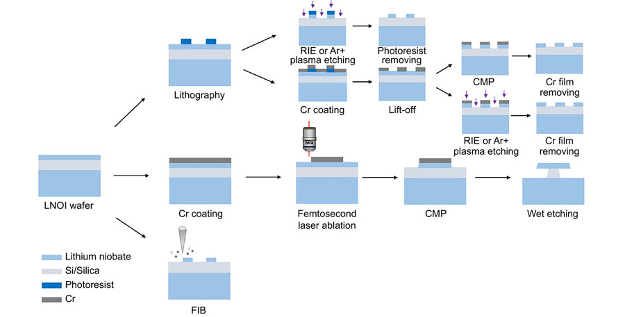
Fig. 1. The main flow chart of fabrication of photonic structure on the LNOI chip: patterned processing; pattern transfer; post-processing
![(a) A schematic of the SHG from the lithium niobate metasurface; (b) Schematic illustration of the process flow of fabrication; (c) SEM image of the fabricated metasurface in which the nanoresonator consists of a truncated pyramid and a residual layer underneath[64]](/richHtml/gdgc/2022/49/10/220093/220093-2.jpg)
Fig. 2. (a) A schematic of the SHG from the lithium niobate metasurface; (b) Schematic illustration of the process flow of fabrication; (c) SEM image of the fabricated metasurface in which the nanoresonator consists of a truncated pyramid and a residual layer underneath[64]
Fig. 3. (a) SEM image of a cylindrical post formed after femtosecond laser ablation; (b) SEM image of the cylindrical post after the FIB milling[70]
Fig. 4. Microring fabricated by UV lithography and RIE, followed by sidewall polishing by the CMP. (a) Schematic illustration of the process flow of fabrication; (b) False-color SEM image of the microring; and enlarged SEM image of the sidewall (c) before and (d) after the CMP[75]
Fig. 5. (a) A schematic of the SHG from the nonlinear lithium niobate metasurface. Left inset gives a typical SEM image of cross section of the metasurface with D=600 nm. Right inset presents the measured second-order susceptibility of the lithium niobate film used in this study; (b) Spectral dependence of SHG efficiencies from metasurfaces[101]
Fig. 6. (a) SPDC from a lithium niobate metasurface: the pump is incident from the substrate side, photon pairs are collected in reflection. Both the pump and the SPDC photons are polarized along the lithium niobate optic axis z; (b) Measured SPDC spectra from quantum optical metasurfaces. Gray stars show the SPDC spectrum from the unpatterned lithium niobate film[112]
Fig. 7. (a) Metasurface driven by Au electrodes. The lower left inset shows the SEM image of the metasurface pillar structure. The lower right inset shows a false-color SEM of several metasurfaces (purple) between the electrodes (yellow); (b) Measured transmission (blue) of a metasurface with radius 135 nm and period 500 nm, normalized by the transmission of an unstructured area. The orange line shows the modulation enhancement, defined as the modulation amplitude of the metasurface divided by the modulation amplitude of an unpatterned area, for an AC voltage of 2 Vpp and 180 kHz[65]
Fig. 8. (a) Schematic of the LiNbO3 on-chip ridge waveguide integrated with a well-designed gradient metasurface for achieving phase-matching-free second harmonic generation; (b) Conceptual diagram of the metasurface-based phase-matching-free second harmonic generation[88]
|
Table 1. Main performance parameters of metasurface SHG

Set citation alerts for the article
Please enter your email address
© Copyright 2018-2021 | Chinese Laser Press. All Rights Reserved 沪ICP备15018463号-20