Abstract
We report a double Q-switched 946 nm laser with a magnesium-oxide-doped (MgO:LN) electro-optic (EO) crystal and a monolayer molybdenum diselenide () saturable absorber (SA). A pulsed laser diode side-pumped long neodymium-doped yttrium aluminum garnet rod () is used as the gain medium. Large pulse energy up to 3.15 mJ and peak power up to 346 kW are generated at the repetition rate of 550 Hz, corresponding to the beam quality factors of , . Monolayer nanosheets applied in the experiment would be a promising SA for a passive Q-switching operation.In recent years, transition metal dichalcogenides (, Mo; , Se), as a new class of two-dimensional (2D) materials, have recently stimulated a great deal of research due to their unique and exotic properties. The bandgap tunability by reducing the layer number or introducing defects[1–4], high carrier mobility, and strong spin–orbit coupling made them appealing materials for various applications in electronics and photonics. Recent investigations have demonstrated that layered molybdenum diselenide () has broadband saturable absorption from 400 to 2100 nm[5] and exhibits nonlinear optical absorption characteristics to generate laser pulses by Q-switching or mode-locking[6–9]. However, reports on and similar materials used as saturable absorbers (SAs) in passively Q-switched/mode-locked lasers occur the most in wavelengths longer than 1 μm[6–9]. Few studies focus on pulsed laser performance in wavelengths shorter than 1 μm.
Near-infrared 946 nm pulsed lasers with short pulse width and high peak power have been widely used in various fields, such as water vapor detection, ozone detection, differential absorption radar, and second harmonic generation[10,11]. In contrast with the generally used neodymium-doped yttrium aluminum garnet (Nd:YAG) crystal for a 1064 nm laser, in which the light stimulation originates from a four-level system (), the typical quasi-three-level model for 946 nm wavelength radiation has a relatively small stimulated emission cross section ( of the cross section of 1064 nm)[12]. This significantly increases the challenge of acquiring large pulse energy at high repetition rates. Moreover, the strong fluorescence photon re-absorption and intrinsic parasitic oscillations lead to a serious thermal effect, which, thus, greatly increases the laser oscillation threshold[13]. In order to suppress the thermal effect and parasitic oscillation, conventional approaches mainly depend on an end-pumped Nd:YAG crystal with a short length[14–16]. The small mode volume and short gain length in an end-pumped short crystal are an effective solution for reducing thermal effects and re-absorption in its counterpart crystal rod (i.e., side-pumped long Nd:YAG crystal rod). However, laser diode (LD) end-pumped short Nd:YAG crystals still suffer bottleneck in larger peak power generation at relatively high repetition rates because of limited gain length and pump beam size. Although the pulse width and pulse energy have been reduced to be shorter than 20 ns and enhanced to a few hundreds of microjoules, the peak power is still confined in a few tens of kilowatts[14–16]. On the other hand, an LD side-pumped Nd:YAG crystal rod has been demonstrated as an effective mechanism for high power and large pulse energy generation. Technically, an LD side-pump can be divided into continuous wave (CW) and pulsed schemes. In CW LD side-pumped 946 nm lasers, thermal effects and parasitic oscillation are drastically amplified due to long gain medium. To overcome this drawback, a good solution is to use pulsed LD side-pumped long Nd:YAG crystal rods. The small duty cycle in pulsed pumping enables considerable reduction of the unwanted thermal effect and parasitic oscillation in a long crystal rod. However, very few investigations by pulsed LD side-pumped Nd:YAG crystals for a 946 nm laser were reported. In fact, our former work has demonstrated this approach as a feasible solution for high energy pulse and high peak power generation[17]. Despite extensive fundamental studies on actively or passively Q-switched operation being reported, there defects still remain, including relatively long pulse width, low pulse energy and peak power, poor pulse stability, and asymmetric waveform[18]. Compared to an actively or passively Q-switching operation, a double Q-switching operation (a combination of both actively and passively Q-switching operations) has been demonstrated as an effective approach to achieve pulses with higher peak power, shorter pulse width, better beam quality, and better pulse waveform symmetry[19–21].
In this Letter, we demonstrate a double Q-switched laser with peak power up to 300 kW at 946 nm. A monolayer SA and an electro-optic (EO) crystal were combined to actively and passively Q-switch the laser simultaneously at a repetition rate of 550 Hz. A pulsed LD side-pumped long Nd:YAG crystal rod is employed to increase the laser gain. In comparison with a CW pumping, the small duty cycle (25%) of the pulsed LD enables effective reduction of the thermal effect and parasitic oscillation that may cause the detuning of the laser. The use of a SA can significantly suppress the pulse width, and, as a consequence, such a Q-switched laser with both passively and actively Q-switching operating could effectively compress the pulse width and acquire higher peak power and better beam quality.
Sign up for Chinese Optics Letters TOC. Get the latest issue of Chinese Optics Letters delivered right to you!Sign up now
The chemical vapor deposition (CVD) method was used to grow the material. The chemical reaction process was carried out in an Ar and gases enriched environment[22,23]. was generated after the reaction of a mixed compound including , , and Se powder precursors in a high temperature quartz tube furnace. The boat containing the powder (250 mg, 99.6%) and the substrates (25 μm thick, ) was placed in the center of the quartz tube, and another boat containing the Se powder (500 mg, 99.6%) was placed in the upstream of the quartz tube. Air was first expelled from the quartz tube by Ar gas with flow rate of 200 standard cubic centimeters per minute (sccm). After one hour, Ar and mixed gases (94% Ar and 6% ) were injected into the quartz tube with a flow rate of 50 sccm, in which acts as catalyst to accelerate the chemical reaction by the equation . Meanwhile, the quartz tube was heated to the growth temperature of 950°C by 30°C/min ramping rate and sustained for 5 min. High quality film samples could be deposited on the substrates during this process. Finally, the film on the substrate was cooled down to room temperature under the Ar environment with a flow rate of approximately 20–30 sccm.
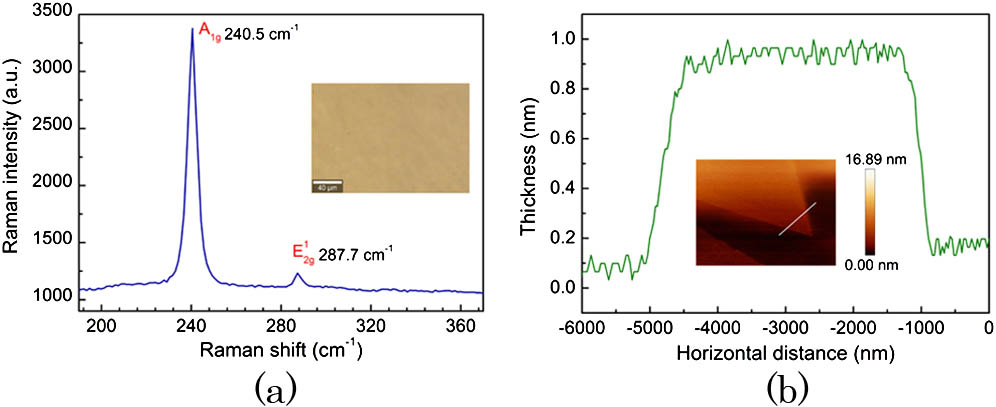
Figure 1(a) shows the Raman spectrum of the fabricated film excited by the 532 nm laser, where two characteristic peaks [ () and ()] were observed. This verifies that the fabricated material is , and the film is made up of a monolayer or a few layers[20,21]. It is noticed that no characteristic peak is shown at around in the spectrum, which is identified as a fingerprint of monolayer , corresponding to the vibration between layers. Figure 1(b) shows the thickness and micro-morphologies of the same film have been measured by atomic force microscopy (AFM). The thickness () of the same film is 0.77 nm, which is consistent with general evaluation of monolayer [24].

Figure 1.(a) Raman spectrum of film. Inset: microscopic morphology of film, scale bar: 40 μm. (b) Morphology (inset) and thickness profile (the white line in the inset) of the film measured by AFM.
The curve in Fig. 2(a) shows a linear absorption spectrum from visible to near-infrared[25]. It is demonstrated that the optical absorption reduced dramatically as the wavelength increases. The linear absorption coefficient () is calculated according to Lambert’s Law , in which is the transmitted light intensity, is the incident light intensity, and is the film thickness. Taking the values of ( at 946 nm) and (0.77 nm) into account, is calculated to be at the incident wavelength of 946 nm. Nonlinear optical properties of the same material were investigated using the open aperture Z-scan method with a femtosecond laser at 1030 nm (340 fs, 100 Hz). As shown in Fig. 2(b), one can observe that the transmission efficiencies of the monolayer film increase with the pulse intensity. The monolayer exhibits a typical saturable absorption at relatively low photon energy of 1.2 eV at 1030 nm, which is less than the band gap (1.55 eV) of monolayer . Similar phenomena have also been reported by other groups[26]. The bandgap reduction caused by crystal defects may provide a proper explanation for such observations. Most of the layered materials used as SAs are in a finite area, and, as such, they could not be considered as an infinite crystal structure. Symmetry broken at the edge of the flakes and unsatisfactory bonds between Mo and Se atoms at the edge might modify the band structure of the atomic planes and relate to edge-states in the film. Moreover, the edge-states effect could become pronounced in the sheets with a large edge to surface area ratio[27]. This suggests that the edge-states might play an important role in defining the band structure of and result in photon density within the bandgap of monolayer [28]. Absorptions with sub-bandgap energy could be permitted, and, thus, the electrons are able to transit from the valence band to these states with reduced energy, which could be saturated to initiate the Q-switching operation for a laser with wavelengths shorter than 1030 nm, such as 946 nm. Theoretical curve fitting was obtained by taking the following equation into account[29]: where is the modulation depth, is the saturation power intensity, is the thickness of monolayer , and is the non-saturable absorption coefficient, which was calculated to be 5.44%. The modulation depth of monolayer film was , and the saturable power density was calculated to be .
Figure 2.(a) Linear absorption spectrum of monolayer film. (b) Normalized nonlinear optical transmittance (blue dots) measured with Z-scan apparatus by using ultrashort pulsed laser (1030 nm, 340 fs) and theoretical fitting (red line) of the monolayer .
Monolayer film was transferred onto glass to form an SA mirror. The preparation procedures can be divided as follows: first, the monolayer film was spin-coated with polymethyl methacrylate (PMMA) for mechanical support, which was then dried in a vacuum oven for 10 min at 100°C. PMMA-coated film was soaked in the NaOH solution () for 30 min at 100°C, to remove the substrate underneath. The remaining PMMA supported film was then washed in deionized water repeatedly to reduce the NaOH residue. The PMMA supported film was then transferred onto a high-reflection (HR) mirror at 946 nm and dried for 10 min at 100°C. Finally, PMMA was dissolved by acetone and isopropanol. An SA mirror with monolayer film was obtained after rinsing the transferred film in deionized water and drying in a vacuum oven for 2 h at 45°C.
The laser schematic is shown in Fig. 3. An Nd:YAG crystal rod (, with 0.5 at.% concentration) is used as the gain medium, pumped by a pulsed 808 nm LD. In addition, traditional crystals such as (BBO), (KDP), (RTP), and (LN) have been extensively used for EO modulators in solid state lasers. Nonetheless, BBO and KDP are easy to deliquesce, RTP is expensive, and LN has low optical damage threshold. In contrast with a traditional LN crystal, MgO:LN has a comparative half-wave voltage of transverse EO modulation, more than two orders of magnitude of optical damage threshold, and lower cost[30]. In the experiment, a half-wave voltage of from an EO driver was transversely loaded between two sides of the double 45° cut-MgO:LN crystal (length × width × thickness 20 mm × 7 mm × 5 mm, 5.5 mol.% MgO doping, 250 MW optical damage threshold). The EO driver has a rising edge shorter than 5 ns and a wide range of pulse repetition rate from 1 Hz to 5 kHz. The double 45° cut-MgO:LN crystal functions as a polarizer, EO modulator, and analyzer. If the high voltage of the EO driver is unstable, it is impossible to ensure that the voltage on the EO crystal is half-wave voltage; so, the extinction ratio of the EO crystal will decrease. This will prolong the turn-off time of the EO crystal and trailing time of the laser pulse, resulting in a longer pulse width and a poorer stability of the single pulse energy and pulse width. Therefore, the EO modulator usually needs to be fine-tuned in the experiment to ensure that the EO crystal can obtain accurate half-wave voltage. The two vertical incidence surfaces were anti-reflection (AR) -coated () at 946 nm, and two 45° cutting surfaces were HR () -coated at 946 nm. The Nd:YAG rod was used to generate 946 nm non-polarized light, which was mutually side-pumped by three 808 nm pulsed LD arrays in 120° angles and water-cooled to 10°C. The two end surfaces were AR () -coated for 1064, 1319, and 946 nm, respectively. The radii of concave curvatures of and were calculated to be 3.0 and 1.0 m, respectively. The formed cavity is . Plano-concave mirror was HR-coated () at 946 nm and AR-coated () at both 1064 and 1319 nm, which can be used as an SA mirror after transferring the monolayer film to its concave surface. The transmittance of output mirror was measured to be 9%. The triggering signals of the pulsed 808 nm LD and EO driver were received from a delay pulse signal generator. The triggering time of the two signals was adjusted to ensure that the transverse half-wave voltage can be synchronized with the 808 nm pulsed LD pumping.
Figure 3.Sketch of the experimental setup (top view). Inset: monolayer SA mirror.
After passing through the double 45° cut-MgO:LN crystal in the case without load voltage, the non-polarized light was split into a bunch of ordinarily (o) polarized light and another bunch of extraordinarily (e) polarized light due to the natural birefringence. All of the polarized beams were parallel to the original non-polarized one, but there were no vertical placements of the output mirror on the outgoing optical path to disable the oscillation of the laser. When the transverse half-wave voltage was abruptly loaded on the double 45° cut-MgO:LN crystal, the refractive indices for the two polarized light beams were varied to different extents due to the EO effect. This leads to unparallel propagation of the o-polarized and e-polarized light after the double 45° cut-MgO:LN crystal. We intentionally put to form a folded cavity with ; in between, the o-polarized light at 946 nm can be extracted via oscillation.
In practical applications of the 946 nm laser, it is often desirable to have the pulse repetition rate as high as possible in order to achieve higher detection speed. In our experiment, when the repetition rate of the pulse LD exceeded 550 Hz, the greatly increased heat accumulation in the Nd:YAG crystal rod caused severe fluorescence photon re-absorption and parasitic oscillations. As a result, the output energy of the 946 nm laser dropped significantly. Reducing the repetition rate of the pulsed LD helps to increase the one-way laser gain and the compressed pulse width, so that the single pulse energy and the peak power of the 946 nm laser increased accordingly. However, it also increases the risk of the monolayer SA being damaged. Therefore, the repetition rate of the pulsed LD is limited to 550 Hz in our experiment. The time interval between two adjacent LD pulses is , and the pulsed LD with a pulse width of 250 μs can fully pump the Nd:YAG crystal rod with an upper laser-level lifetime of .
At the LD pump energy of 305 mJ and 550 Hz pulse repetition rate, detailed laser performance comparisons of the three Q-switched operations were summarized in Table 1. When the MgO:LN crystal and the pulsed LD are triggered synchronously in the cavity without insertion of the SA mirror, an actively Q-switching operation could be initiated by the EO modulator. 5.48 mJ pulse energy, 20.2 ns pulse width, 271 kW peak power, and 550 Hz repetition rate were acquired, respectively. Likewise, the passively Q-switching operation was achieved when the SA mirror was positioned as a reflection mirror, and the transverse high voltage of was always loaded between the two sides of the double 45° cut-MgO:LN EO crystal. When the pulse frequency of the pulsed LD is fixed to 550 Hz, the pulse train containing the sub-pulses was obtained. The pulse width of each pulse train is about 230 μs, corresponding to a 550 Hz repetition rate. The repetition rate change of the passively Q-switching operation with the LD pump energy is shown in Fig. 4. The repetition rate of the sub-pulses increased with the LD pump energy. At the LD pump energy of 305 mJ, each pulse train contains sub-pulses, corresponding to a 152 kHz repetition rate, as shown in the inset of the Fig. 4. The single pulse energy, pulse width, and peak power of the sub-pulse were , , and , respectively. The double Q-switching operation was obtained when the EO Q-switcher was turned on together with an SA integrated into the reflection mirror, and, thus, active and passive optical modulation would dominate the laser pulse generation. The maximum output of 3.15 mJ, peak power of 346 kW, pulse width of 9.1 ns, and repetition rate of 550 Hz were obtained.
| | | | | Peak-to-peak Instability | | |
|---|
| Q-switching Mode | Maximum Single Pulse Energy (mJ) | Pulse Width (ns) | Peak Power (kW) | Duration | Energy | Spectral Linewidth (nm) | Symmetrical Factor |
|---|
| EO-actively | 5.48 | 20.2 | 271 | ±4.66% | ±5.78% | 0.245 | 0.38 |
| MoSe2-passively | 0.106 | 51.5 | 2.06 | ±6.18% | ±8.14% | 0.197 | 0.92 |
| Double | 3.15 | 9.1 | 346 | ±2.87% | ±3.42% | 0.173 | 0.87 |
Table 1. Actively EO, Passively MoSe2 and Double Q-switched Laser Performances
Figure 4.Pulse peak power versus incident pump energy of LD. Inset: sub-pulses in a pulse train for passively Q-switching operation.
The single pulse energy, pulse width, peak power, symmetrical factor, and spectral linewidth of the 946 nm pulsed laser at 550 Hz for actively, passively, and double Q-switching operations were summarized in Figs. 5(a)–5(d), respectively. The peak power of the laser pulse can be approximately calculated by formula , where is single pulse energy, and is pulse width. The peak-to-peak instability can be calculated by , in which can be single pulse energy or pulse width. The symmetric factor of the pulse profile can be calculated by formula , where and represent the rising and falling edge times of the pulse profile, respectively.
Figure 5.Output performances of 946 nm pulse laser for actively EO, passively, and double Q-switching operation. (a) Single pulse energy, (b) pulse width, (c) peak power, and (d) symmetrical factor.
It was observed that pulse width of the double Q-switched laser was further compressed from 51.2 to 9.1 ns as the operation converts from active to passive and then to double Q-switching, as shown in Figs. 6(a), 6(b), and 6(c). Compared with the actively EO Q-switched laser and passively Q-switched laser, the reduction ratio of the pulse width was more than 50% and 75%, respectively. The peak power was increased from 271 to 346 kW.
Figure 6.Output pulse profiles of (a) actively EO, (b) passively, and (c) double Q-switching operation.
The insertion of the monolayer film introduces intracavity optical loss by valence band absorption. This contributes to the increase of the laser oscillation threshold and the decrease of pulse width. However, the longitudinal modes far from the central wavelength are suppressed because their gain is smaller than the threshold. Since the pulse width of the double Q-switched laser is very short, only a few single longitudinal modes close to the central wavelength are obtained because of larger gain. Thus, the monolayer SA functions as a filter to select longitudinal modes. The compression of the double Q-switched laser spectral linewidth from 0.245 to 0.173 nm is a result of the filtering, as shown in Fig. 7. The reduced longitudinal mode number improves the stability of the double Q-switched laser. In comparison with the actively EO Q-switched laser, the peak-to-peak instability of the pulse width and single pulse energy were reduced from to and from to , respectively. In comparison with the passively Q-switched laser and actively EO Q-switched laser, peak power was increased from 2.06 to 346 kW, and the peak-to-peak instabilities of the pulse width and single pulse energy were reduced from to and from to , respectively.
Figure 7.Linewidth of 946 nm pulse laser with actively EO, passively, and double Q-switching operation.
It is found that the pulse symmetry of the double Q-switched laser is much better than that of the sole actively Q-switched laser. This can be explained as follows: when the SA was inserted in the cavity, the Q-switched pulses were filtered via the intensity dependent absorption property. The pulse wings along the rising edge and falling edge were filtered by the SA, resulting in a more symmetric pulse profile, but it cannot completely eliminate the pulse tailing phenomenon in the actively Q-switched laser. Obviously, the falling edge of the actively Q-switched laser is far longer than the passively Q-switched laser, as shown in Figs. 6(a) and 6(b). The symmetrical factor of 0.87 in the double Q-switching operation is larger than that of 0.38 in the single actively Q-switching operation and smaller than that of 0.92 in the single passively Q-switching operation.
Figures 8(a), 8(b), and 8(c) show the 2D and three dimensional (3D) far-field intensity distributions measured with a laser beam quality analyzer of the actively EO, passively, and double Q-switching operation, respectively. It is clearly observable that the use of the SA helps to improve the beam quality of the 946 nm laser. As the operation converted from actively EO Q-switching to passively Q-switching, then, to double Q-switching, the beam quality factor was reduced from to and then to again.
Figure 8.2D and 3D near-field beam profiles of (a) actively EO, (b) passively, and (c) double Q-switching operation.
These results demonstrate that the direct bandgap structure of the monolayer film is beneficial to the passively Q-switching operation of the pulsed laser. In our double Q-switched laser cavity, the monolayer film worked as an SA, and a filter can significantly compress the pulse width and spectral linewidth, which is the key approach to increase the peak power and to optimize the beam quality and output light stability.
In summary, we demonstrate a SA-based double Q-switching operation of the 946 nm solid state pulse laser. In our experiment, such monolayer film with a modulation depth of 0.98% is fabricated by the CVD method and then embedded on a surface of the mirror with HR coating at 946 nm. When inserting the monolayer SA into an EO Q-switched 946 nm cavity with double 45° cut-MgO:LN, stable 946 nm laser pulses with single pulse energy of 3.15 mJ, pulse width of 9.1 ns, peak power of 346 kW, and pulse waveform symmetry factor of 0.87 were obtained at a 550 Hz pulse repetition rate. The corresponding peak-to-peak instabilities of the pulse width and single pulse energy were and , respectively. Meanwhile, the beam quality factor (, ) was measured. Our experimental results show that the double Q-switching operation with a double 45° cut-MgO:LN EO Q-switcher and monolayer film SA can generate shorter laser pulse, higher peak power, higher symmetry, and higher stability for a pulse laser shorter than 1 μm.
References
[1] S. X. Wang, H. H. Yu, H. J. Zhang, A. Z. Wang, M. W. Zhao, Y. X. Chen, L. M. Mei, J. Y. Wang. Adv. Mater., 26, 3538(2014).
[2] I. H. Baek, H. W. Lee, S. Bae, B. H. Hong, Y. H. Ahn, D.-I. Yeom, F. Rotermund. Appl. Phys. Express, 5, 032701(2012).
[3] V. Nguyen, J. H. Si, L. H. Yan, X. Hou. Carbon, 95, 659(2015).
[4] Z. Q. Li, C. Cheng, N. N. Dong, C. Romero, Q. M. Lu, J. Wang, J. R. Vázquez de Aldana, Y. Tan, F. Chen. Photon. Res., 5, 406(2017).
[5] Z. Q. Luo, Y. Y. Li, M. Zhong, Y. Z. Huang, X. J. Wan, J. Peng, J. Weng. Photon. Res., 3, A79(2015).
[6] R. I. Woodward, R. C. Howe, T. H. Runcorn, G. Hu, F. Torrisi, E. J. Kelleher, T. Hasan. Opt. Express, 23, 20051(2015).
[7] B. H. Chen, X. Y. Zhang, K. Wu, H. Wang, J. Wang, J. P. Chen. Opt. Express, 23, 26723(2015).
[8] J. Koo, J. Park, J. Lee, Y. M. Jhon, J. H. Lee. Opt. Express, 24, 10575(2016).
[9] Z. C. Tiu, H. Ahmad, A Zarei, S.W. Harun. Chin. Opt. Lett., 14, 041901(2016).
[10] X. Y. Wang, S. G. Li, H. L. Chen, G. Y. Wang, Y. Y. Zhao. Opt. Quantum Electron., 48, 1(2016).
[11] S. P. Ng, J. I. Mackenzie. Laser Phys., 22, 494(2012).
[12] O. Kimmelma, M. Kaivola, L. Tittonen, S. Buchter. Opt. Commun., 273, 496(2007).
[13] H. P. Cheng, T. L. Huang, C. L. Sung, C. Y. Cho, H. C. Liang, Y. F. Chen. Opt. Lett., 42, 2224(2017).
[14] R. Yan, X. Yu, X. Li, D. Chen, J. Yu. Appl. Phys. B Laser Opt., 108, 591(2012).
[15] J. Huang, X. H. Hu, W. B. Chen. Chin. Opt. Lett., 13, 021402(2015).
[16] L. Deyra, I. Martial, J. Didierjean, F. Balembois, P. Georges. Opt. Lett., 38, 3013(2013).
[17] Y. X. Sun, Y. Bai, D. Li, L. Hou, B. Bai, Y. Z. Gong, L. L. Yu, J. T. Bai. Optics Express, 25, 21037(2017).
[18] V. Dashkevich, P. Shpak, S. Voitikov, R. Chulkov, A. Grabtchikov, E. Cheshev, M. El-Desouki, V. Orlovich. Opt. Commun., 351, 1(2015).
[19] T. W. Chen, K. C. Chang, J. C. Chen, J. H. Lin, M. D. Wei. Appl. Opt., 53, 3459(2014).
[20] T. Li, S. Z. Zhao, Z. Zhuo, K. J. Yang, G. Q. Li, D. C. Li. J. Opt. Soc. Am. B, 26, 1146(2009).
[21] K. Cheng, S. Z. Zhao, K. J. Yang, G. Q. Li, D. C. Li, G Zhang, B. Zhao, Y. G. Wang. Opt. Laser Technol., 44, 903(2012).
[22] Y. H. Chang, W. J. Zhang, Y. H. Zhu, Y. Han, J. Pu, J. K. Chang, W. T. Hsu, J. K. Huang, C. L. Hsu, M. H. Chiu, T. Takenobu, H. N. Li, C. I. Wu, W. H. Chang. ACS Nano, 8, 8582(2014).
[23] J. C. Shaw, H. L. Zhou, Y. Chen, N. O. Weiss, Y. Liu, Y. Huang, X. F. Duan. Nano Res., 7, 511(2014).
[24] Y. J. Zhang, Q. F. Gong, L. Li, H. C. Yang, Y. G. Li, Q. B. Wang. Nano Res., 8, 1108(2015).
[25] A. R. Beal, J. C. Knights, W. Y. Liang. J. Phys. C Solid State Phys., 5, 3540(1972).
[26] P. Rivera, J. R. Schaibley, A. M. Jones, J. S. Ross, S. F. Wu, G. Aivazian, P. Klement, K. Seyler, G. Clark, N. J. Ghimire, J. Q. Yan, D. G. Mandrus, W. Yao, X. D. Xu. Nat. Commun., 6, 6242(2015).
[27] C. B. Roxlo, M. Daage, A. F. Ruppert, R. R. Chianelli. J. Catal., 100, 176(1986).
[28] W. Zhou, X. L. Zou, S. Najmaei, Z. Liu, Y. M. Shi, J. Kong, J. Lou, P. M. Ajayan, B. I. Yakobson, J. C. Idrobo. Nano Lett., 13, 2615(2013).
[29] S. F. Zhang, N. N. Dong, N. McEvoy, M. O’Brien, S. Winters, N. C. Berner, C. Y. Yim, Y. X. Li, X. Y. Zhang, Z. H. Chen, L. Zhang, G. S. Duesberg, J. Wang. ACS Nano, 9, 7142(2015).
[30] R. Zhou, T. L. Zhang, E. B. Li, X. Ding, Z. Q. Cai, B. G. Zhang, W. Q. Wen, P. Wang, J. Q. Yao. Opt. Express, 13, 10115(2005).